


AMD Geode™ SC3200 Processor Data Book 241
Core Logic Module - SMI Status and ACPI Registers - Function 1
32581C
Offset 22h-23h Second Level ACPI PME/SMI Status Register (RC) Reset Value: 0000h
The bits in this register contain second level of SMI status reporting. Top level is reported in F1BAR0+I/O Offset 00h/02h[2].
Reading this register clears the status at both the second and top levels.
A read-only “Mirror” version of this register exists at F1BAR0+I/O Offset 20h. If the value of the register must be read without clearing the
SMI source (and consequently de-asserting SMI), F1BAR0+I/O Offset 20h can be read instead.
15:6 Reserved. Always reads 0.
5 ACPI BIOS SMI Status. Indicates whether or not an SMI was caused by ACPI software raising an event to BIOS software.
0: No.
1: Yes.
To enable SMI generation, set F1BAR1+I/O Offset 0Ch[2] to 1, and F1BAR1+I/O Offset 0Fh[0] to 1.
4 PLVL3 SMI Status. Indicates whether or not an SMI was caused by a read of the ACPI PLVL3 register (F1BAR1+I/O Offset
05h).
0: No.
1: Yes.
To enable SMI generation, set F1BAR1+I/O Offset 18h[11] to 1 (default).
3 Reserved.
2 SLP_EN SMI Status. Indicates whether or not an SMI was caused by a write of 1 to the ACPI SLP_EN bit (F1BAR1+I/O
Offset 0Ch[13]).
0: No.
1: Yes.
To enable SMI generation, set F1BAR1+I/O Offset 18h[9] to 1 (default).
1 THT_EN SMI Status. Indicates whether or not an SMI was caused by a write of 1 to the ACPI THT_EN bit (F1BAR1+I/O
Offset 00h[4])
0: No.
1: Yes.
To enable SMI generation, set F1BAR1+I/O Offset 18h[8] to 1 (default).
0 SMI_CMD SMI Status. Indicates whether or not an SMI was caused by a write to the ACPI SMI_CMD register (F1BAR1+I/
O Offset 06h).
0: No.
1: Yes.
A write to the ACPI SMI_CMD register always generates an SMI.
Offset 24h-27h External SMI Register (R/W) Reset Value: 00000000h
Note: EXT_SMI[7:0] are external SMIs, meaning external to the Core Logic module.
Bits [23:8] of this register contain second level of SMI status reporting. Top level status is reported in F1BAR0+I/O Offset 00h/
02h[10]. Reading bits [23:16] clears the second and top levels. If the value of the status bits must be read without clearing the
SMI source (and consequently de-asserting SMI), bits [15:8] can be read instead.
31:24 Reserved. Must be set to 0.
23 EXT_SMI7 SMI Status. (Read to Clear) Indicates whether or not an SMI was caused by assertion of EXT_SMI7.
0: No.
1: Yes.
To enable SMI generation, set bit 7 to 1.
22 EXT_SMI6 SMI Status. (Read to Clear) Indicates whether or not an SMI was caused by an assertion of EXT_SMI6
0: No.
1: Yes.
To enable SMI generation, set bit 6 to 1.
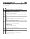
Table 6-33. F1BAR0+I/O Offset: SMI Status Registers (Continued)
Bit Description