AMD Geode™ SC3200 Processor Data Book 253
Core Logic Module - SMI Status and ACPI Registers - Function 1
32581C
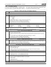
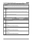
Offset 16h GPWIO Data Register (R/W) Reset Value: 00h
This register contains the direct values of the GPWIO2-GPWIO0 pins. Write operations are valid only for bits defined as outputs. Reads
from this register read the last written value if the pin is an output. The pins are configured as inputs or outputs in F1BAR1+I/O Offset
15h.
7:4 Reserved. Must be set to 0.
3 Reserved.
2 GPWIO2_DATA. Reflects the level of GPWIO2.
0: Low.
1: High.
A fixed high-to-low or low-to-high transition (debounce period) of 31 µs exists in order for GPWIO2 to be recognized.
1 GPWIO1_DATA. Reflects the level of GPWIO1.
0: Low.
1: High.
See F1BAR1+I/O Offset 07h[3] for debounce information.
0 GPWIO0_DATA. Reflects the level of GPWIO0.
0: Low.
1: High.
See F1BAR1+I/O Offset 07h[3] for debounce information.
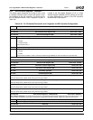
Offset 17h Reserved Reset Value: 00h
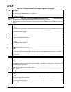
Offset 18h-1Bh ACPI SCI_ROUTING Register (R/W) Reset Value: 00000F00h
31:17 Reserved.
16 PCTL_DELAYEN. Allow staggered delays on the activation and deactivation of the power control pins PWRCNT1,
PWRCNT2, and ONCTL# by 2 ms each.
0: Disable. (Default)
1: Enable.
15:12 Reserved. Must be set to 0.
11 PLVL3_SMIEN. Allow SMI generation when the PLVL3 Register (F1BAR1+I/O Offset 05h) is read.
0: Disable.
1: Enable. (Default)
Top level SMI status is reported at F1BAR0+I/O Offset 00h/02h[2].
Second level SMI status is reported at F1BAR0+I/O Offset 20h/22h[4].
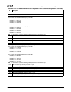
10 Reserved. Must be set to 0.
9 SLP_SMIEN. Allow SMI generation when the SLP_EN bit (F1BAR1+I/O Offset 0Ch[13]) is set.
0: Disable.
1: Enable. (Default)
Top level SMI status is reported at F1BAR0+I/O Offset 00h/02h[2].
Second level SMI status is reported at F1BAR0+I/O Offset 20h/22h[2].
8 THT_SMIEN. Allow SMI generation when the THT_EN bit (F1BAR1+I/O Offset 00h[4]) is set.
0: Disable.
1: Enable. (Default)
Top level SMI status is reported at F1BAR0+I/O Offset 00h/02h[2].
Second level SMI status is reported at F1BAR0+I/O Offset 20h/22h[1].
7:4 Reserved. Must be set to 0.
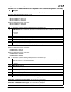
Table 6-34. F1BAR1+I/O Offset: ACPI Support Registers (Continued)
Bit Description


