AMD Geode™ SC3200 Processor Data Book 89
SuperI/O Module
32581C
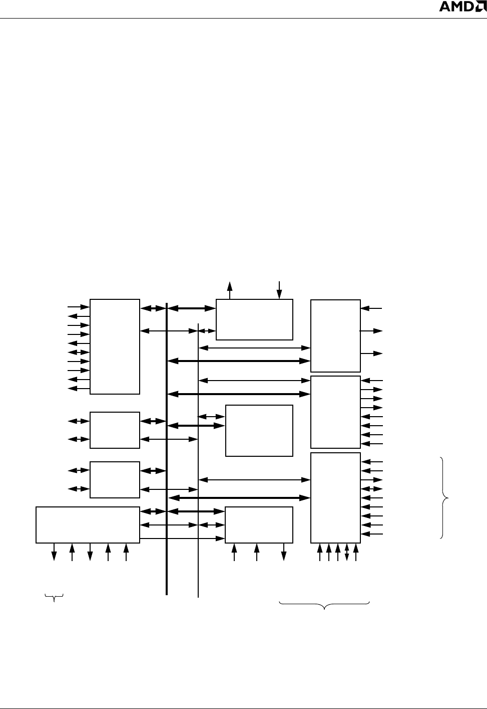
5.2 Module Architecture
The SIO module comprises a collection of generic func-
tional blocks. Each functional block is described in detail
later in this chapter. The beginning of this chapter
describes the SIO structure and provides all device specific
information, including special implementation of generic
blocks, system interface and device configuration.
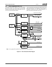
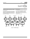
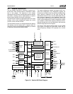
The SIO module is based on eight logical devices, the host
interface, and a central configuration register set, all built
around a central, internal 8-bit bus.
The host interface serves as a bridge between the external
ISA interface and the internal bus. It supports 8-bit I/O
read, 8-bit I/O write and 8-bit DMA transactions, as defined
in Personal Computer Bus Standard P996.
The central configuration register set supports ACPI com-
pliant PnP configuration. The configuration registers are
structured as a subset of the Plug and Play Standard Reg-
isters, defined in Appendix A of the Plug and Play ISA
Specification Version 1.0a by Intel and Microsoft®. All sys-
tem resources assigned to the functional blocks (I/O
address space, DMA channels and IRQ lines) are config-
ured in, and managed by, the central configuration register
set. In addition, some function-specific parameters are con-
figurable through this unit and distributed to the functional
blocks through special control signals.
The source of the device internal clocks is the 48 MHz
clock signal or through the 32.768 KHz crystal with an
internal frequency multiplier. RTC operates on a 32 KHz
clock.
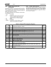
Figure 5-2. Detailed SIO Block Diagram
SIN1
SOUT1
IRRX1/SIN3
IRTX/SOUT3
PWUREQ
Parallel
Serial
Port 1
and Control
Registers
System
Wakeup
Port
DACK0-3
DRQ0-3
Internal Bus
Host
Control Signals
IRQ1-12,14-15
SIN2
SOUT2
RTS2#
DTR2#/BOUT2
CTS2
Serial
Port 2
RI2#
V
BAT
V
SB
Configuration
TC
Infrared
Interface
Real-Time Clock (RTC)
CONFIG
CLKIN
MR
X1C/X1
X2C
D[7:0]
IOCHRDY
IOWR#
IORD#
A[15:0]
AEN
ZWS#
ALARM
ACCESS.
AB1C
AB1D
AB2C
AB2D
SDATA_IN2
ACK#
AFD#/DSTRB#
BUSY/WAIT#
ERR#
INIT#
PD[7:0]
PE
SLCT
SLIN#/ASTRB#
STB#/WRITE#
DTR#/BOUT1
Internal
Internal
Internal Signals
Internal
RI2#
DCD2#
DSR2#
bus 1
ACCESS.
bus 2
Signal
Communication
Port/Serial Port 3
Signals


