


58 AMD Geode™ SC3200 Processor Data Book
Signal Definitions
32581C
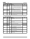
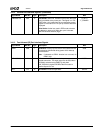
3.4.8 Low Pin Count (LPC) Bus Interface Signals
Signal Name Ball No. Type Description Mux
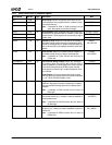
LAD3 L29 I/O LPC Address-Data. Multiplexed command,
address, bidirectional data, and cycle status.
GPIO35
LAD2 L30 GPIO34
LAD1 L31 GPIO33
LAD0 M28 GPIO32
LDRQ# L28 I LPC DMA Request. Encoded DMA request for
LPC interface.
Note: If LDRQ# function is selected but not
used, tie LDRQ# high.
GPIO36
LFRAME# K31 O LPC Frame. A low pulse indicates the beginning
of a new LPC cycle or termination of a broken
cycle.
GPIO37
LPCPD# K28 O LPC Power-Down. Signals the LPC device to pre-
pare for power shut-down on the LPC interface.
GPIO38/IRRX2
SERIRQ J31 I/O Serial IRQ. The interrupt requests are serialized
over a single signal, where each IRQ level is deliv-
ered during a designated time slot.
Note: If SERIRQ function is selected but not
used, tie SERIRQ high.
GPIO39
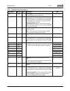
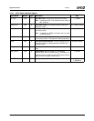
3.4.9 IDE Interface Signals
Signal Name Ball No. Type Description Mux
IDE_RST# AA1 O IDE Reset. This signal resets all the devices that are
attached to the IDE interface.
TFTDCK
IDE_ADDR2 U2 O IDE Address Bits. These address bits are used to
access a register or data port in a device on the IDE bus.
TFTD4
IDE_ADDR1 AE1 TFTD2
IDE_ADDR0 AD3 TFTD3
IDE_DATA[15:0] See
Table 3-3
on page
40.
I/O IDE Data Lines. IDE_DATA[15:0] transfers data to/from
the IDE devices.
The IDE interface is
muxed with the TFT
interface. See Table
3-5 on page 45 for
details.
IDE_IOR0# Y4 O IDE I/O Read Channels 0 and 1. IDE_IOR0# is the read
signal for Channel 0 and IDE_IOR1# is the read signal
for Channel 1. Each signal is asserted at read accesses
to the corresponding IDE port addresses.
TFTD10
IDE_IOR1# D28 O GPIO6+DTR2#/
BOUT2+SDTEST5#
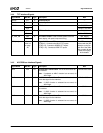
IDE_IOW0# AD2 O IDE I/O Write Channels 0 and 1. IDE_IOW0# is the
write signal for Channel 0. IDE_IOW1# is the write signal
for Channel 1. Each signal is asserted at write accesses
to corresponding IDE port addresses.
TFTD9
IDE_IOW1# C28 O GPIO9+DCD2#+
SDTEST2
IDE_CS0# AF2 O IDE Chip Selects 0 and 1. These signals are used to
select the command block registers in an IDE device.
TFTD5
IDE_CS1# P2 O TFTDE