


AMD Geode™ SC3200 Processor Data Book 57
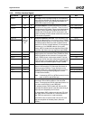
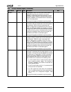
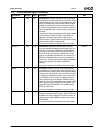
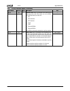
Signal Definitions
32581C
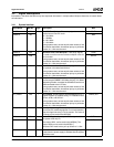
3.4.7 Sub-ISA Interface Signals
Signal Name Ball No. Type Description Mux
A[23:0] See Table
3-3 on
page 40.
O Address Lines AD[23:0]
D15 See Table
3-3 on
page 40.
I/O Data Bus STOP#
D14 IRDY#
D13 TRDY#
D12 PAR
D11 C/BE3#
D10 C/BE2#
D9 C/BE1#
D8 C/BE0#
D[7:0] AD[31:24]
BHE# E4 O Byte High Enable. With A0, defines byte
accessed for 16 bit wide bus cycles.
DEVSEL#
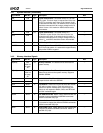
IOCS1# D10 O I/O Chip Selects GPIO1+TFTD12
N30 AB1D+GPIO1
IOCS0# A10 GPIO17+TFTDCK
ROMCS# C30 O ROM or Flash ROM Chip Select BOOT16 (Strap)
DOCCS# A9 O DiskOnChip or NAND Flash Chip Select GPIO20+TFTD0
N31 AB1C+GPIO20
TRDE# D11 O Transceiver Data Enable Control. Active low for
Sub-ISA data transfers. The signal timing is as fol-
lows:
• In a read cycle, TRDE# has the same timing as
RD#.
• In a write cycle, TRDE# is asserted (to active
low) at the time WR# is asserted. It continues
being asserted for one PCI clock cycle after
WR# has been negated, then it is negated.
GPIO0
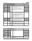
RD# B8 O Memory or I/O Read. Active on any read cycle. CLKSEL0 (Strap)
WR# B9 O Memory or I/O Write. Active on any write cycle. ---
IOR# D9 O I/O Read. Active on any I/O read cycle. DOCR#+GPIO14
IOW# A8 O I/O Write. Active on any I/O write cycle. DOCW#+GPIO15
DOCR# D9 O DiskOnChip or NAND Flash Read. Active on any
memory read cycle to DiskOnChip.
IOR#+GPIO14
DOCW# A8 O DiskOnChip or NAND Flash Write. Active on
any memory write cycle to DiskOnChip.
IOW#+GPIO15
IRQ9 AA3 I Interrupt 9 Request Input. Active high.
Note: If IRQ9 function is selected but not used,
tie IRQ9 low.
IDE_DATA6
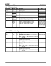
IOCHRDY C9 I I/O Channel Ready
Note: If IOCHRDY function is selected but not
used, tie IOCHRDY high.
GPIO19+INTC#