AMD Geode™ SC3200 Processor Data Book 277
Core Logic Module - X-Bus Expansion Interface - Function 5
32581C
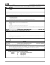
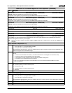
Index 1Ch-1Fh Base Address Register 3 - F5BAR3 (R/W) Reset Value: 00000000h
Reserved. Reserved for possible future use by the Core Logic module.
Configuration of this register is programmed through the F5BAR3 Mask Register (F5 Index 4Ch).
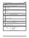
Index 20h-23h Base Address Register 4 - F5BAR4 (R/W) Reset Value: 00000000h
Reserved. Reserved for possible future use by the Core Logic module.
Configuration of this register is programmed through the F5BAR4 Mask Register (F5 Index 50h).
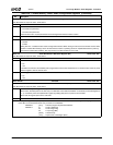
Index 24h-27h Base Address Register 5 - F5BAR5 (R/W) Reset Value: 00000000h
Reserved. Reserved for possible future use by the Core Logic module.
Configuration of this register is programmed through the F5BAR5 Mask Register (F5 Index 54h).
Index 28h-2Bh Reserved Reset Value: 00h
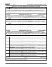
Index 2Ch-2Dh Subsystem Vendor ID (RO) Reset Value: 100Bh
Index 2Eh-2Fh Subsystem ID (RO) Reset Value: 0505h
Index 30h-3Fh Reserved Reset Value: 00h
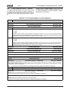
Index 40h-43h F5BAR0 Mask Address Register (R/W) Reset Value: FFFFFFC1h
To use F5BAR0, the mask register should be programmed first. The mask register defines the size of F5BAR0 and whether the
accessed offset registers are memory or I/O mapped.
Note: Whenever a value is written to this mask register, F5BAR0 must also be written (even if the value for F5BAR0 has not
changed).
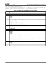
Memory Base Address Register (Bit 0 = 0)
31:4 Address Mask. Determines the size of the BAR.
— Every bit that is a 1 is programmable in the BAR.
— Every bit that is a 0 is fixed 0 in the BAR.
Since the address mask goes down to bit 4, the smallest memory region is 16 bytes, however, the PCI specification sug-
gests not using less than a 4 KB address range.
3 Prefetchable. Indicates whether or not the data in memory is prefetchable. This bit should be set to 1 only if all the following
are true:
— There are no side-effects from reads (i.e., the data at the location is not changed as a result of the read).
— The device returns all bytes regardless of the byte enables.
— Host bridges can merge processor writes into this range without causing errors.
— The memory is not cached from the host processor.
0: Data is not prefetchable. This value is recommended if one or more of the above listed conditions is not true.
1: Data is prefetchable.
2:1 Type.
00: Located anywhere in the 32-bit address space
01: Located below 1 MB
10: Located anywhere in the 64-bit address space
11: Reserved
0 This bit must be set to 0, to indicate memory base address register.
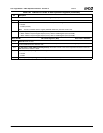
I/O Base Address Register (Bit 0 = 1)
31:2 Address Mask. Determines the size of the BAR.
— Every bit that is a 1 is programmable in the BAR.
— Every bit that is a 0 is fixed 0 in the BAR.
Since the address mask goes down to bit 2, the smallest I/O region is 4 bytes, however, the PCI Specification suggests not
using less than a 4 KB address range.
1 Reserved. Must be set to 0.
0 This bit must be set to 1, to indicate an I/O base address register.
Table 6-39. F5: PCI Header Registers for X-Bus Expansion (Continued)
Bit Description


