AMD Geode™ SC3200 Processor Data Book 265
Core Logic Module - Audio Registers - Function 3
32581C
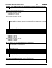
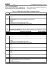
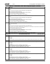
4 Audio Bus Master 2 SMI Status. Indicates if an SMI was caused by an event occurring on Audio Bus Master 2.
0: No.
1: Yes.
SMI generation is enabled when Audio Bus Master 2 is enabled (F3BAR0+Memory Offset 30h[0] = 1). An SMI is then gen-
erated when the End of Page bit is set in the SMI Status Register (F3BAR0+Memory Offset 31h[0] = 1). The End of Page bit
must be cleared before this bit can be cleared.
3 Audio Bus Master 1 SMI Status. Indicates if an SMI was caused by an event occurring on Audio Bus Master 1.
0: No.
1: Yes.
SMI generation is enabled when Audio Bus Master 1 is enabled (F3BAR0+Memory Offset 28h[0] = 1). An SMI is then gen-
erated when the End of Page bit is set in the SMI Status Register (F3BAR0+Memory Offset 29h[0] = 1). The End of Page bit
must be cleared before this bit can be cleared.
2 Audio Bus Master 0 SMI Status. Indicates if an SMI was caused by an event occurring on Audio Bus Master 0.
0: No.
1: Yes.
SMI generation is enabled when Audio Bus Master 0 is enabled (F3BAR0+Memory Offset 20h[0] = 1). An SMI is then gen-
erated when the End of Page bit is set in the SMI Status Register (F3BAR0+Memory Offset 21h[0] = 1). The End of Page bit
must be cleared before this bit can be cleared.
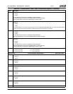
1 Codec Serial or GPIO Interrupt SMI Status. Indicates if an SMI was caused by a serial or GPIO interrupt from codec.
0: No.
1: Yes.
SMI generation enabling for codec serial interrupt: F3BAR0+Memory Offset 08h[23] = 1.
SMI generation enabling for codec GPIO interrupt: F3BAR0+Memory Offset 00h[30] = 1.
0 I/O Trap SMI Status. Indicates if an SMI was caused by an I/O trap.
0: No.
1: Yes.
The next level (third level) of SMI status reporting is at F3BAR0+Memory Offset 14h.
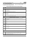
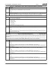
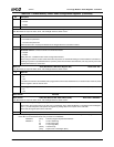
Offset 14h-17h I/O Trap SMI and Fast Write Status Register (RO/RC) Reset Value: 00000000h
Note: For the four SMI status bits (bits [13:10]), if the activity was a fast write to an even address, no SMI is generated regardless of
the DMA, MPU, or Sound Card status. If the activity was a fast write to an odd address, an SMI is generated but bit 13 is set to
a 1.
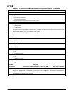
31:24 Fast Path Write Even Access Data. (Read Only) This bit field contains the data from the last Fast Path Write Even
access. These bits change only on a fast write to an even address.
23:16 Fast Path Write Odd Access Data. (Read Only) This bit field contains the data from the last Fast Path Write Odd access.
These bits change on a fast write to an odd address, and also on any non-fast write.
15 Fast Write A1. (Read Only) This bit contains the A1 value for the last Fast Write access.
14 Read or Write I/O Access. (Read Only) Indicates if the last trapped I/O access was a read or a write.
0: Read.
1: Write.
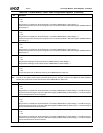
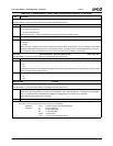
13 Sound Card or FM Trap SMI Status. (Read to Clear) Indicates if an SMI was caused by a trapped I/O access to the
Sound Card or FM I/O Trap.
0: No.
1: Yes. (See the note included in the general description of this register above.)
Fast Path Write must be enabled, F3BAR0+Memory Offset 18h[11] = 1, for the SMI to be reported here. If Fast Path Write is
disabled, the SMI is reported in bit 10 of this register.
This is the third level of SMI status reporting.
Second level SMI status is reported at F3BAR0+Memory Offset 10h/12h[0].
Top level is reported at F1BAR0+I/O Offset 00h/02h[1].
SMI generation enabling is at F3BAR0+Memory Offset 18h[2].
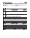
Table 6-38. F3BAR0+Memory Offset: Audio Configuration Registers (Continued)
Bit Description


