AMD Geode™ SC3200 Processor Data Book 343
Video Processor Module - Video Processor Registers - Function 4
32581C
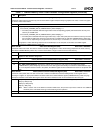
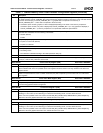
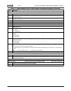
Offset 90h-93h Video Request Register (R/W) Reset Value: 001B0017h
31:28 Reserved. Set to 0.
27:16 VIDEO_X_REQ (Video Horizontal Request). Determines the horizontal (pixel) location at which to start requesting video
data out of the video FIFO. This value is calculated according to the following formula:
Value = Desired screen position + (H_TOTAL – H_SYNC_END) – 2.
15:11 Reserved
10:0 VIDEO_Y_REQ (Video Vertical Request). Determines the line number at which to start requesting video data out of the
video FIFO. This value is calculated according to the following formula:
Value = Desired screen position + (V_TOTAL – V_SYNC_END) + 1.
Offset 94h-97h Alpha Watch Register (RO) Reset Value: 00000000h
Alpha values may be automatically incremented/decremented for successive frames. This register can be used to read the alpha values
that are being used in the current frame.
31:24 Reserved.
23:16 ALPHA3_VAL (Value for Alpha Window 3).
15:8 ALPHA2_VAL (Value for Alpha Window 2).
7:0 ALPHA1_VAL (Value for Alpha Window 1).
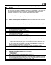
Offset 98h-3FFh Reserved
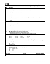
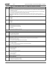
Offset 400h-403h Video Processor Display Mode Register (R/W) Reset Value: 00000000h
Selects various Video Processor modes.
31 Video FIFO Underflow (Empty).
0: No underflow has occurred.
1: Underflow has occurred.
Write 1 to reset this bit.
30 Video FIFO OverFlow (Full).
0: No overflow has occurred.
1: Overflow has occurred.
Write 1 to reset this bit.
29 Reserved. Write as read.
28 Reserved. Write as read.
27:4 Reserved. Set to 0.
3 Reserved. Write as read.
2 Note: Reserved. Write as read.
1:0 VID_SEL (Video Select). Selects the source of the video data.
00: GX1 module.
10: VIP block.
01: Reserved.
11: Reserved.
The GX1 module’s video clock must be active at all times, regardless of the source of video input.
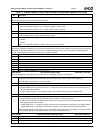
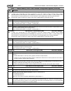
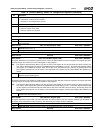
Offset 404h-407h Reserved Reset Value: 00000000h
Offset 408h-40Bh Video Processor Test Mode Register (R/W) Reset Value: 00000000h
31:0 Reserved.
Offset 40Ch-41Fh Reserved
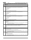
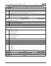
Table 7-7. F4BAR0+Memory Offset: Video Processor Configuration Registers (Continued)
Bit Description


