


22 AMD Geode™ SC3200 Processor Data Book
Architecture Overview
32581C
2.1.2 Fast-PCI Bus
The GX1 module communicates with the Core Logic mod-
ule via a Fast-PCI bus that can work at up to 66 MHz. The
Fast-PCI bus is internal for the SC3200 and is connected to
the General Configuration Block (see Section 4.0 on page
69 for details on the General Configuration Block).
This bus supports seven bus masters. The requests
(REQs) are fixed in priority. The seven bus masters in order
of priority are:
1) VIP
2) IDE Channel 0
3) IDE Channel 1
4) Audio
5) USB
6) External REQ0#
7) External REQ1#
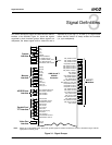
2.1.3 Display
The GX1 module generates display timing, and controls
internal VSYNC and HSYNC signals of the Video Proces-
sor module.
The GX1 module interfaces with the Video Processor via a
video data bus and a graphics data bus.
• Video data. The GX1 module uses the core clock,
divided by 2 or 4 (typically 100 - 133 MHz). It drives the
video data using this clock. Internal signals VID_VAL
and VID_RDY are used as data-flow handshake signals
between the GX1 module and the Video Processor.
• Graphics data. The GX1 module uses the internal
signal DCLK, supplied by the PLL of the Video
Processor, to drive the 18-bit graphics-data bus of the
Video Processor. Each six bits of this bus define a
different color. Each of these 6-bit color definitions is
expanded (by adding two zero LSB lines) to form an 8-
bit bus, at the Video Processor.
For more information about the GX1 module’s interface to
the Video Processor, see the “Display Controller” chapter
in the AMD Geode™ GX1 Processor Data Book.
2.2 Video Processor Module
The Video Processor provides high resolution and graphics
for a TFT/DSTN interface. The following subsections pro-
vide a summary of how the Video Processor interfaces with
the other modules of the SC3200. For detailed information
about the Video Processor, see Section 7.0 "Video Proces-
sor Module" on page 309.
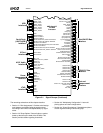
2.2.1 GX1 Module Interface
The Video Processor is connected to the GX1 module in
the following way:
• The Video Processor’s DOTCLK output signal is used as
the GX1 module’s DCLK input signal.
• The GX1 module’s PCLK output signal is used as the
GFXCLK input signal of the Video Processor.
2.2.2 Video Input Port
The Video Input Port (VIP) within the Video Processor con-
tains a standard interface that is typically connected to a
media processor or TV encoder. The clock is supplied by
the externally connected device; typically at 27 MHz.
Video input can be sent to the GX1 module’s video frame
buffer (Capture Video mode) or can be used directly (Direct
Video mode).
2.2.3 Core Logic Module Interface
The Video Processor interfaces to the Core Logic module
for accessing PCI function configuration registers.
2.3 Core Logic Module
The Core Logic module is described in detail in Section 6.0
"Core Logic Module" on page 139.
The Core Logic module is connected to the Fast-PCI bus. It
uses signal AD28 as the IDSEL for all PCI configuration
functions except for USB which uses AD29.
2.3.1 Other Core Logic Module Interfaces
The following interfaces of the Core Logic module are
implemented via external balls of the SC3200. Each inter-
face is listed below with a reference to the descriptions of
the relevant balls.
• IDE: See Section 3.4.9 "IDE Interface Signals" on page
58.
• AC97: See Section 3.4.14 "AC97 Audio Interface
Signals" on page 63.
• PCI: See Section 3.4.6 "PCI Bus Interface Signals" on
page 53.
• USB: See Section 3.4.10 "Universal Serial Bus (USB)
Interface Signals" on page 59. The USB function uses
signal AD29 as the IDSEL for PCI configuration.
• LPC: See Section 3.4.8 "Low Pin Count (LPC) Bus Inter-
face Signals" on page 58.