


344 AMD Geode™ SC3200 Processor Data Book
Video Processor Module - Video Processor Registers - Function 4
32581C
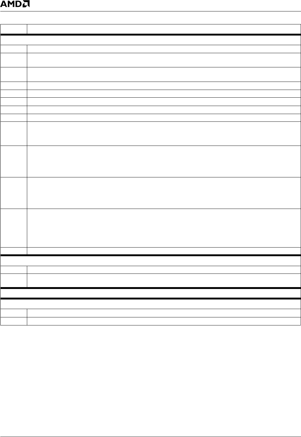
Offset 420h-423h GenLock Register (R/W) Reset Value: 00000000h
31:24 Reserved. Must be set to 0.
23 ODD_TO (Odd Field Time Out). Indicates CGENTO0 (F4BAR0+Memory Offset 43Ch[15:0]) has expired. This bit can be
reset by writing 1 to it.
22 EVEN_TO (Even Field Time Out). Indicates CGENTO1 (F4BAR0+Memory Offset 43Ch[31:16]) has expired. This bit can
be reset by writing 1 to it.
21:9 Reserved.
8 Reserved. Set to 0.
7 Reserved. Set to 0.
6 Reserved. Set to 0.
5 Reserved. Set to 0.
4 GENLOCK_TOUT_EN (GenLock Timeout Enable).
0: Disable.
1: Enable timeout.
3 VIP_VSYNC_EDGE_SEL (VIP VSYNC Edge Select). Selects which edge of the VSYNC signal should be synchronized
with VIP.
0: Rising edge.
1: Falling edge.
2 GX1_VSYNC_EDGE_SEL (GX1 VSYNC Edge Select). Selects which edge of the VSYNC signal should be synchronized
with the GX1 module.
0: Rising edge.
1: Falling edge.
1 CT_GENLOCK_EN (Enable Continuous GenLock Function).
0: The continuous GenLock function is disabled.
1: Enable locking (i.e., synchronization) of the GX1 VSYNC with the VIP VSYNC on every VSYNC (i.e., continuous lock-
ing).
Note: If bit 0 (SG_GENLOCK_EN) = 1, it overrides the value of this bit.
0 Reserved. Set to 0.
Offset 424h-427h GenLock Delay Register (R/W) Reset Value: 00000000h
31:21 Reserved.
20:0 GENLOCK_DEL (GenLock Delay). Indicates the delay (in 27 MHz clocks) between the VIP VSYNC and the GX1 module’s
Display Controller VSYNC.
Offset 428h-43Bh Reserved
Offset 43Ch-43Fh Continuous GenLock Timeout Register (R/W) Reset Value: 1FFF1FFFh
31:16 CGENTO1 (Even Field Continuous GenLock Timeout).
15:0 CGENTO0 (Odd Field Continuous GenLock Timeout).
Table 7-7. F4BAR0+Memory Offset: Video Processor Configuration Registers (Continued)
Bit Description