


AMD Geode™ SC3200 Processor Data Book 183
Core Logic Module - Register Summary
32581C
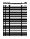
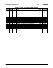
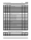
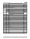
Table 6-24. F5: PCI Header Registers for X-Bus Expansion Support Summary
F5 Index
Width
(Bits) Type Name
Reset
Value
Reference
(Table 6-39)
00h-01h 16 RO Vendor Identification Register 100Bh Page 276
02h-03h 16 RO Device Identification Register 0505h Page 276
04h-05h 16 R/W PCI Command Register 0000h Page 276
06h-07h 16 RO PCI Status Register 0280h Page 276
08h 8 RO Device Revision ID Register 00h Page 276
09h-0Bh 24 RO PCI Class Code Register 068000h Page 276
0Ch 8 RO PCI Cache Line Size Register 00h Page 276
0Dh 8 RO PCI Latency Timer Register 00h Page 276
0Eh 8 RO PCI Header Type Register 00h Page 276
0Fh 8 RO PCI BIST Register 00h Page 276
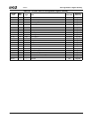
10h-13h 32 R/W Base Address Register 0 (F5BAR0) — Sets the base address for
the X-Bus Expansion support registers (summarized in
Table 6-25.)
00000000h Page 276
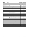
14h-17h 32 R/W Base Address Register 1 (F5BAR1) — Reserved for possible
future use by the Core Logic module.
00000000h Page 276
18h-1Bh 32 R/W Base Address Register 2 (F5BAR2) — Reserved for possible
future use by the Core Logic module.
00000000h Page 276
1Ch-1Fh 32 R/W Base Address Register 3 (F5BAR3) — Reserved for possible
future use by the Core Logic module.
00000000h Page 277
20h-23h 32 R/W Base Address Register 4 (F5BAR4) — Reserved for possible
future use by the Core Logic module.
00000000h Page 277
24h-27h 32 R/W Base Address Register 5 (F5BAR5) — Reserved for possible
future use by the Core Logic module.
00000000h Page 277
28h-2Bh --- --- Reserved 00h Page 277
2Ch-2Dh 16 RO Subsystem Vendor ID 100Bh Page 277
2Eh-2Fh 16 RO Subsystem ID 0505h Page 277
30h-3Fh --- --- Reserved 00h Page 277
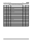
40h-43h 32 R/W F5BAR0 Base Address Register Mask FFFFFFC1h Page 277
44h-47h 32 R/W F5BAR1 Base Address Register Mask 00000000h Page 278
48h-4Bh 32 R/W F5BAR2 Base Address Register Mask 00000000h Page 278
4Ch-4Fh 32 R/W F5BAR3 Base Address Register Mask 00000000h Page 278
50h-53h 32 R/W F5BAR4 Base Address Register Mask 00000000h Page 278
54h-57h 32 R/W F5BAR5 Base Address Register Mask 00000000h Page 278
58h 8 R/W F5BARx Initialized Register 00h Page 278
59h-FFh --- --- Reserved xxh Page 278
60h-63h 32 R/W Scratchpad for Chip Number 00000000h Page 278
64h-67h 32 R/W Scratchpad for Configuration Block Address 00000000h Page 279
68h-FFh --- --- Reserved 00h Page 279
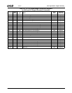
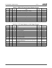
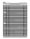
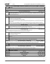
Table 6-25. F5BAR0: I/O Control Support Registers Summary
F5BAR0+
I/O Offset
Width
(Bits) Type Name
Reset
Value
Reference
(Table 6-40)
00h-03h 32 R/W I/O Control Register 1 010C0007h Page 280
04h-07h 32 R/W I/O Control Register 2 00000002h Page 281
08h-0Bh 32 R/W I/O Control Register 3 00009000h Page 281