


AMD Geode™ SC3200 Processor Data Book 249
Core Logic Module - SMI Status and ACPI Registers - Function 1
32581C
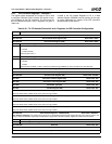
Offset 0Fh ACPI_BIOS_EN Register (R/W) Reset Value: 00h
7:2 Reserved. Must be set to 0.
1 BIOS_RLS (BIOS Release). (Write Only) When this bit is asserted, allow the BIOS to release control of the global lock.
0: Disable.
1: Enable.
This is a write only bit and reads of this bit always return a 0.
To generate an SCI, the BIOS writes the BIOS_RLS bit which in turn sets the GBL_STS bit (F1BAR1+I/O Offset 08h[5]) and
raises a PME. For the PME to generate an SCI, set GBL_EN (F1BAR1+I/O Offset 0Ah[5] to 1).
0 BIOS_EN (BIOS Enable). When this bit is asserted, allow SMI generation by ACPI software via writes to GBL_RLS
(F1BAR1+I/O Offset 0Ch[2]).
0: Disable.
1: Enable
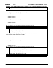
Offset 10h-11h GPE0_STS — General Purpose Event 0 PME/SCI Status Register (R/W) Reset Value: xxxxh
Notes: 1) This is the top level of PME/SCI status reporting. There is no second level except for bit 3 (GPIOs) where the next level of
status is reported at F0BAR0+I/O Offset 0Ch/1Ch.
2) If SCI generation is not desired, the status bits are still set by the described conditions and can be used for monitoring pur-
poses.
15:12 Reserved. Must be set to 0.
11 Reserved.
10 GPWIO2_STS. Indicates if PME was caused by activity on GPWIO2.
0: No.
1: Yes.
Write 1 to clear.
For the PME to generate an SCI:
1) Ensure that GPWIO2 is enabled as an input (F1BAR1+I/O Offset 15h[2] = 0)
2) Set F1BAR1+I/O Offset 12h[10] = 1 and F1BAR1+I/O Offset 0Ch[0] = 1. (See Note 2 in the general description of this
register above.)
If F1BAR1+I/O Offset 15h[6] = 1 it overrides these settings and GPWIO2 generates an SMI and the status is reported in
F1BAR0+00h/02h[0].
9 GPWIO1_STS. Indicates if PME was caused by activity on GPWIO1.
0: No.
1: Yes.
Write 1 to clear.
For the PME to generate an SCI:
1) Ensure that GPWIO1 is enabled as an input (F1BAR1+I/O Offset 15h[1] = 0)
2) Set F1BAR1+I/O Offset 12h[9] = 1 and F1BAR1+I/O Offset 0Ch[0] = 1. (See Note 2 in the general description of this
register above.)
If F1BAR1+I/O Offset 15h[5] = 1 it overrides these settings and GPWIO1 generates an SMI and the status is reported in
F1BAR0+00h/02h[0].
8 GPWIO0_STS. Indicates if PME was caused by activity on GPWIO0.
0: No.
1: Yes.
Write 1 to clear.
For the PME to generate an SCI:
1) Ensure that GPWIO0 is enabled as an input (F1BAR1+I/O Offset 15h[0] = 0)
2) Set F1BAR1+I/O Offset 12h[8] = 1 and F1BAR1+I/O Offset 0Ch[0] = 1. (See Note 2 in the general description of this
register above).
If F1BAR1+I/O Offset 15h[4] = 1 it overrides these settings and GPWIO0 generates an SMI and the status is reported in
F1BAR0+00h/02h[0].
Table 6-34. F1BAR1+I/O Offset: ACPI Support Registers (Continued)
Bit Description