266 AMD Geode™ SC3200 Processor Data Book
Core Logic Module - Audio Registers - Function 3
32581C
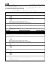
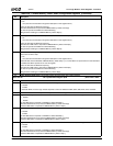
12 DMA Trap SMI Status. (Read to Clear) Indicates if an SMI was caused by a trapped I/O access to the DMA I/O Trap.
0: No.
1: Yes. (See the note included in the general description of this register above.)
This is the third level of SMI status reporting.
Second level SMI status is reported at F3BAR0+Memory Offset 10h/12h[0].
Top level is reported at F1BAR0+I/O Offset 00h/02h[1].
SMI generation enabling is at F3BAR0+Memory Offset 18h[8:7].
11 MPU Trap SMI Status. (Read to Clear) Indicates if an SMI was caused by a trapped I/O access to the MPU I/O Trap.
0: No.
1: Yes. (See the note included in the general description of this register above.)
This is the third level of SMI status reporting.
Second level of SMI status is reported at F3BAR0+Memory Offset 10h/12h[0].
Top level is reported at F1BAR0+I/O Offset 00h/02h[1].
SMI generation enabling is at F3BAR0+Memory Offset 18h[6:5].
10 Sound Card or FM Trap SMI Status. (Read to Clear) Indicates if an SMI was caused by a trapped I/O access to the
Sound Card or FM I/O Trap.
0: No.
1: Yes. (See the note included in the general description of this register above.)
Fast Path Write must be disabled, F3BAR0+Memory Offset 18h[11] = 0, for the SMI to be reported here. If Fast Path Write
is enabled, the SMI is reported in bit 13 of this register.
This is the third level of SMI status reporting.
Second level of SMI status is reported at F3BAR0+Memory Offset 10h/12h[0].
Top level is reported at F1BAR0+I/O Offset 00h/02h[1].
SMI generation enabling is at F3BAR0+Memory Offset 18h[2].
9:0 X-Bus Address (Read Only). This bit field] contains the captured ten bits of X-Bus address.
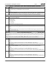
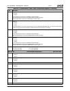
Offset 18h-19h I/O Trap SMI Enable Register (R/W )Reset Value: 0000h
15:12 Reserved. Must be set to 0.
11 Fast Path Write Enable. Fast Path Write (an SMI is not generated on certain writes to specified addresses).
0: Disable.
1: Enable.
In Fast Path Write, the Core Logic module responds to writes to addresses: 388h, 38Ah, 38B, 2x0h, 2x2h, and 2x8h.
10:9 Fast Read. These two bits hold part of the response that the Core Logic module returns for reads to several I/O locations.
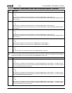
8 High DMA I/O Trap. If this bit is enabled and an access occurs at I/O Port C0h-DFh, an SMI is generated.
0: Disable.
1: Enable.
Top level SMI status is reported at F1BAR0+I/O Offset 00h/02h[1].
Second level SMI status is reported at F3BAR0+Memory Offset 10h/12h[0].
Third level SMI status is reported at F3BAR0+Memory Offset 14h[12].
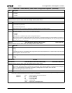
7 Low DMA I/O Trap. If this bit is enabled and an access occurs at I/O Port 00h-0Fh, an SMI is generated.
0: Disable.
1: Enable.
Top level SMI status is reported at F1BAR0+I/O Offset 00h/02h[1].
Second level SMI status is reported at F3BAR0+Memory Offset 10h/12h[0].
Third level SMI status is reported at F3BAR0+Memory Offset 14h[12].
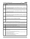
6 High MPU I/O Trap. If this bit is enabled and an access occurs at I/O Port 330h-331h, an SMI is generated.
0: Disable.
1: Enable.
Top level SMI status is reported at F1BAR0+I/O Offset 00h/02h[1].
Second level SMI status is reported at F3BAR0+Memory Offset 10h/12h[0].
Third level SMI status is reported at F3BAR0+Memory Offset 14h[11].
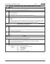
Table 6-38. F3BAR0+Memory Offset: Audio Configuration Registers (Continued)
Bit Description


