


AMD Geode™ SC3200 Processor Data Book 335
Video Processor Module - Video Processor Registers - Function 4
32581C
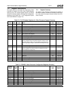
Offset 14h-17h Video Color Key Register (R/W) Reset Value: 00000000h
Provides the video color key. The color key can be used to allow irregular shaped overlays of graphics onto video, or video onto graph-
ics, within a scaled video window.
31:24 Reserved.
23:0 VID_CLR_KEY (Video Color Key). The video color key is a 24-bit RGB or YUV value.
• If the COLOR_CHROMA_SEL bit (F4BAR0+Memory Offset 04h[20]) = 0:
— The video pixel is selected within the target window if the corresponding graphics pixel matches the color key. The
color key in an RGB value.
• If the COLOR_CHROMA_SEL bit (F4BAR0+Memory Offset 04h[20]) = 1:
— The video pixel is selected within the target window only if it (the video pixel) does not match the color key. The color
key is usually an RGB value. However, if both the CSC_for VIDEO and GV_SEL bits (F4BAR0+Memory Offset 4Ch
bits 10 and 13, respectively) are programmed to 0, the color key is a YUV value (i.e., video is not converted to RGB).
The graphics or video data being compared can be masked prior to the compare via the Video Color Mask register
(described in F4BAR0+Memory Offset 18h).
Offset 18h-1Bh Video Color Mask Register (R/W) Reset Value: 00000000h
Provides the video color mask. This value is used to mask bits of the graphics or video stream being compared to the video color key
(described in F4BAR0+Memory Offset 14h). It can be used to allow a range of values to serve as the color key.
31:24 Reserved.
23:0 VID_CLR_MASK (Video Color Mask). This mask is a 24-bit value. Zeros in the mask cause the corresponding bits in the
graphics or video stream to be ignored.
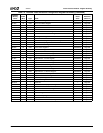
Offset 1Ch-1Fh Palette (Gamma Correction RAM) Address Register (R/W) Reset Value: xxxxxxxxh
31:8 Reserved.
7:0 PAL_ADDR (Palette Address). Specifies the address to be used for the next access to the Palette Data register
(F4BAR0+Memory Offset 20h[31:8]). Each access to the data register automatically increments the Palette Address regis-
ter. If non-sequential access is made to the palette, the address register must be loaded between each non-sequential data
block.
Offset 20h-23h Palette (Gamma Correction RAM) Data Register (R/W) Reset Value: xxxxxxxxh
Provides the video palette data. The data can be read or written to the Gamma Correction RAM (palette) via this register. Prior to
accessing this register, an appropriate address should be loaded to the Palette Address register (F4BAR0+Memory Offset 1Ch[7:0]).
Subsequent accesses to the Palette Data register cause the internal address counter to be incremented for the next cycle.
31:8 PAL_DATA (Palette Data). Contains the read or write data for a Gamma Correction RAM (palette).
Blue[7:0] = Bits [31:24]
Green[7:0] = Bits [23:16]
Red[7:0] = Bits [15:8]
Note: When a read or write to the Gamma Correction RAM occurs, the previous output value is held for one additional
DOTCLK period. This effect should go unnoticed during normal operation.
7:0 Reserved.
Offset 24h-27h Reserved
Table 7-7. F4BAR0+Memory Offset: Video Processor Configuration Registers (Continued)
Bit Description