98 AMD Geode™ SC3200 Processor Data Book
SuperI/O Module
32581C
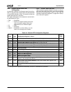
5.4.2.2 LDN 01h - System Wakeup Control
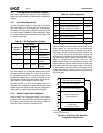
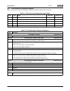
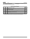
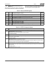
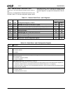
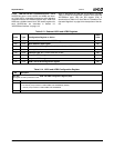
Table 5-8 lists registers that are relevant to the configura-
tion of System Wakeup Control (SWC). These registers are
described earlier in Table 5-3 "Standard Configuration Reg-
isters" on page 93.
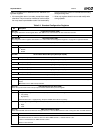
Table 5-8. Relevant SWC Registers
Index Type Configuration Register or Action
Reset
Value
30h R/W
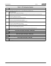
Activate. When bit 0 is cleared, the registers of this logical device are not accessible.
1
00h
60h R/W Base Address MSB register. 00h
61h R/W Base Address LSB register. Bits [3:0] (for A[3:0]) are RO, 0000b. 00h
70h R/W Interrupt Number. (For routing the internal PWUREQ signal.) 00h
71h R/W Interrupt Type. Bit 1 is R/W. Other bits are RO. 03h
74h RO Report no DMA assignment. 04h
75h RO Report no DMA assignment. 04h
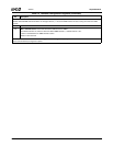
1. The logical device registers are maintained, and all wakeup detection mechanisms are functional.


