386 AMD Geode™ SC3200 Processor Data Book
Electrical Specifications
32581C
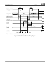
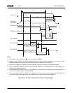
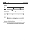
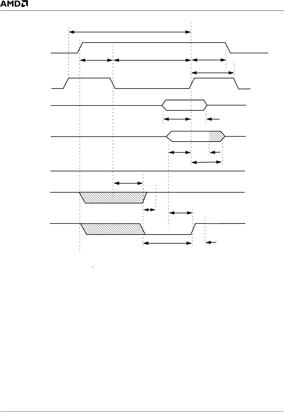
Figure 9-25. PIO Data Transfer to/from Device Timing Diagram
ADDR valid
1
WRITE IDE_DATA[15:0]
READ IDE_DATA[15:0]
t
0
t
1
t
2
t
9
t
2i
t
3
t
5
t
6z
t
6
t
A
t
4
t
C
t
RD
t
B
t
C
IDE_IOR0#
IDE_IOW0#
IDE_IORDY0
2,3
IDE_IORDY0
2,4
IDE_IORDY0
2,5
Notes:
1) Device address consists of signals I
DE_CS[0:1]# and IDE_ADDR[2:0].
2) Negation of IDE_IORDY[0:1] is used to extend the PIO cycle. The determination of whether or not the cycle is to be
extended is made by the host after t
A
from the assertion of IDE_IOR[0:1]# or IDE_IOW[0:1]#.
3) Device never negates IDE_IORDY[0:1]. Devices keep IDE_IORDY[0:1] released, and no wait is generated.
4) Device negates IDE_IORDY[0:1] before t
A
but causes IDE_IORDY[0:1] to be asserted before t
A
.
IDE_IORDY[0:1] is
released, and no wait is generated.
5) Device negates IDE_IORDY[0:1] before t
A
. IDE_IORDY[0:1] is released prior to negation and may be asserted for no
more than 5 ns before release. A wait is generated.
6) The cycle completes after IDE_IORDY[0:1] is reasserted. For cycles where a wait is generated and IDE_IOR[0:1]# is
asserted, the device places read data on IDE_DATA[15:0] for t
RD
before asserting IDE_IORDY[0:1].


