AMD Geode™ SC3200 Processor Data Book 203
Core Logic Module - Bridge, GPIO, and LPC Registers - Function 0
32581C
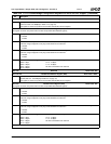
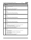
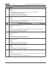
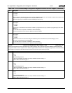
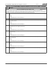
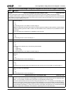
Index 82h Power Management Enable Register 3 (R/W) Reset Value: 00h
7 Video Access Trap. If this bit is enabled and an access occurs in the video address range (sets bit 0 of the GX1 module’s
PSERIAL register), an SMI is generated.
0: Disable.
1: Enable.
Top level SMI status is reported at F1BAR0+I/O Offset 00h/02h[0].
Second level SMI status is reported at F0 Index 86h/F6h[7].
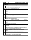
6 User Defined Device 3 (UDEF3) Access Trap. If this bit is enabled and an access occurs in the programmed address
range, an SMI is generated. UDEF3 address programming is at F0 Index C8h (Base Address register) and CEh (Control
register).
0: Disable.
1: Enable.
Top level SMI status is reported at F1BAR0+I/O Offset 00h/02h[9].
Second level SMI status is reported at F1BAR0+I/O Offset 04h/06h[4].
5 User Defined Device 2 (UDEF2) Access Trap. If this bit is enabled and an access occurs in the programmed address
range, an SMI is generated. UDEF2 address programming is at F0 Index C4h (Base Address register) and CDh (Control
register).
0: Disable.
1: Enable.
Top level SMI status is reported at F1BAR0+I/O Offset 00h/02h[9].
Second level SMI status is reported at F1BAR0+I/O Offset 04h/06h[3].
4 User Defined Device 1 (UDEF1) Access Trap. If this bit is enabled and an access occurs in the programmed address
range, an SMI is generated. UDEF1 address programming is at F0 Index C0h (base address register), and CCh (control
register).
0: Disable.
1: Enable.
Top level SMI status is reported at F1BAR0+I/O Offset 00h/02h[9].
Second level SMI status is reported at F1BAR0+I/O Offset 04h/06h[2].
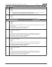
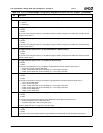
3 Keyboard/Mouse Access Trap.
0: Disable.
1: Enable.
If this bit is enabled and an access occurs in the address ranges listed below, an SMI is generated.
— Keyboard Controller: I/O Ports 060h/064h.
— COM1: I/O Port 3F8h-3FFh (if F0 Index 93h[1:0] = 10 this range is included).
— COM2: I/O Port 2F8h-2FFh (if F0 Index 93h[1:0] = 11 this range is included).
Top level SMI status is reported at F1BAR0+I/O Offset 00h/02h[0].
Second level SMI status is reported at F0 Index 86h/F6h[3].
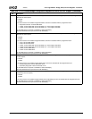
2 Parallel/Serial Access Trap.
0: Disable.
1: Enable.
If this bit is enabled and an access occurs in the address ranges listed below, an SMI is generated.
— LPT1: I/O Port 3BCh-3BEh.
— LPT2: I/O Port 378h-37Fh.
— COM1: I/O Port 3F8h-3FFh (if F0 Index 93h[1:0] = 10 this range is excluded).
— COM2: I/O Port 2F8h-2FFh (if F0 Index 93h[1:0] = 11 this range is excluded).
— COM3: I/O Port 3E8h-3EFh.
— COM4: I/O Port 2E8h-2EFh.
Top level SMI status is reported at F1BAR0+I/O Offset 00h/02h[0].
Second level SMI status is reported at F0 Index 86h/F6h[2].
Table 6-29. F0: PCI Header/Bridge Configuration Registers for GPIO and LPC Support (Continued)
Bit Description


