


AMD Geode™ SC3200 Processor Data Book 327
Video Processor Module - Register Summary
32581C
7.3 Register Descriptions
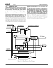
The register space for accessing and configuring the Video
Processor is located in the Core Logic Chipset Register
Space (F0-F5). The Chipset Register Space is accessed
via the PCI interface using the PCI Type One Configuration
Mechanism (see Section 6.3.1 "PCI Configuration Space
and Access Methods" on page 173).
7.3.1 Register Summary
The tables in this subsection summarize the registers of
the Video Processor. Included in the tables are the regis-
ter’s reset values and page references where the bit for-
mats are found.
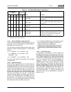
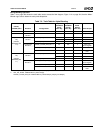
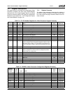
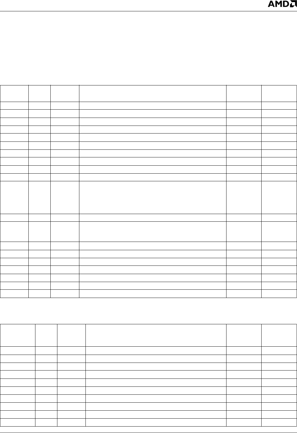
Table 7-3. F4: PCI Header Registers for Video Processor Support Summary
F4 Index
Width
(Bits) Type Name
Reset
Value
Reference
(Table 7-6)
00h-01h 16 RO Vendor Identification Register 100Bh Page 330
02h-03h 16 RO Device Identification Register 0504h Page 330
04h-05h 16 R/W PCI Command Register 0000h Page 330
06h-07h 16 RO PCI Status Register 0280h Page 330
08h 8 RO Device Revision ID Register 01h Page 330
09h-0Bh 24 RO PCI Class Code Register 030000h Page 330
0Ch 8 RO PCI Cache Line Size Register 00h Page 330
0Dh 8 RO PCI Latency Timer Register 00h Page 330
0Eh 8 RO PCI Header Type Register 00h Page 330
0Fh 8 RO PCI BIST Register 00h Page 330
10h-13h 32 R/W Base Address Register 0 (F4BAR0). Sets the base address for the
memory-mapped Video Configuration Registers within the Video
Processor. Refer to Table 7-7 on page 332 for programming infor-
mation regarding the register offsets accessed through this regis-
ter.
00000000h Page 330
14h-17h 32 R/W Base Address Register 1 (F4BAR1). Reserved. 00000000h Page 330
18h-1Bh 32 R/W Base Address Register 2 (F4BAR2). Sets the base address for the
memory-mapped VIP (Video Interface Port) Registers (summa-
rized in Table 7-8 on page 345).
00000000h Page 330
1Ch-2Bh -- -- Reserved 00h Page 330
2Ch-2Dh 16 RO Subsystem Vendor ID 100Bh Page 330
2Eh-2Fh 16 RO Subsystem ID 0504h Page 330
30h-3Bh -- -- Reserved 00h Page 330
3Ch 8 R/W Interrupt Line Register 00h Page 330
3Dh 8 R/W Interrupt Pin Register 03h Page 331
3Eh-FFh --- --- Reserved 00h Page 331
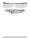
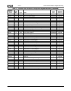
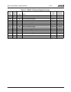
Table 7-4. F4BAR0: Video Processor Configuration Registers Summary
F4BAR0+
Memory
Offset
Width
(Bits) Type Name
Reset
Value
Reference
(Table 7-7)
00h-03h 32 R/W Video Configuration Register 00000000h Page 332
04h-07h 32 R/W Display Configuration Register x0000000h Page 333
08h-0Bh 32 R/W Video X Position Register 00000000h Page 334
0Ch-0Fh 32 R/W Video Y Position Register 00000000h Page 334
10h-13h 32 R/W Video Upscaler Register 00000000h Page 334
14h-17h 32 R/W Video Color Key Register 00000000h Page 335
18h-1Bh 32 R/W Video Color Mask Register 00000000h Page 335
1Ch-1Fh 32 R/W Palette Address Register xxxxxxxxh Page 335
20h-23h 32 R/W Palette Data Register xxxxxxxxh Page 335
24h-27h 32 RO Reserved --- Page 335