


AMD Geode™ SC3200 Processor Data Book 51
Signal Definitions
32581C
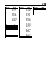
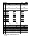
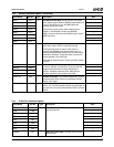
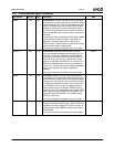
DQM7 AB31 O Data Mask Control Bits. During memory read cycles,
these outputs control whether SDRAM output buffers are
driven on the MD bus or not. All DQM signals are
asserted during read cycles.
During memory write cycles, these outputs control
whether or not MD data is written into SDRAM.
DQM[7:0] connect directly to the [DQM7:0] pins of each
DIMM connector.
---
DQM6 AG29 ---
DQM5 AK21 ---
DQM4 AL15 ---
DQM3 AC31 ---
DQM2 AG30 ---
DQM1 AH23 ---
DQM0 AL11 ---
CKEA AL22 O Clock Enable. These signals are used to enter Suspend/
power-down mode. CKEA is used with CS[1:0]#.
If CKE goes low when no read or write cycle is in
progress, the SDRAM enters power-down mode. To
ensure that SDRAM data remains valid, the self-refresh
command is executed. To exit this mode, and return to
normal operation, drive CKE high.
These signals should have an external pull-down resistor
of 33 KΩ.
---
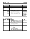
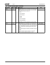
SDCLK3 V29 O SDRAM Clocks. SDRAM uses these clocks to sample
all control, address, and data lines. To ensure that the
Suspend mode functions correctly, SDCLK3 and
SDCLK1 should be used with CS1#. SDCLK2 and
SDCLK0 should be used together with CS0#.
---
SDCLK2 AA28 ---
SDCLK1 W29 ---
SDCLK0 AJ21 ---
SDCLK_IN AJ27 I SDRAM Clock Input. The SC3200 samples the memory
read data on this clock. Works in conjunction with the
SDCLK_OUT signal.
---
SDCLK_OUT AK28 O SDRAM Clock Output. This output is routed back to
SDCLK_IN. The board designer should vary the length of
the board trace to control skew between SDCLK_IN and
SDCLK.
---
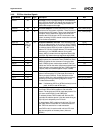
3.4.2 Memory Interface Signals (Continued)
Signal Name Ball No. Type Description Mux
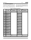
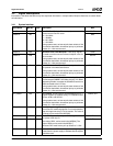
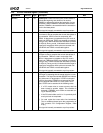
3.4.3 Video Port Interface Signals
Signal Name Ball No. Type Description Mux
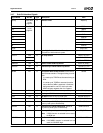
VPD7 G31 I Video Port Data. The data is input from the CCIR-
656 video decoder.
---
VPD6 H28 ---
VPD5 H29 ---
VPD4 H30 ---
VPD3 H31 ---
VPD2 J28 ---
VPD1 J29 ---
VPD0 J30 ---
VPCKIN F31 I Video Port Clock Input. The clock input from the
video decoder.
---