216 AMD Geode™ SC3200 Processor Data Book
Core Logic Module - Bridge, GPIO, and LPC Registers - Function 0
32581C
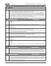
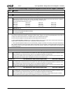
Index BBh RTC Index Shadow Register (RO) Reset Value: xxh
7:0 RTC Index Shadow. The RTC Shadow register contains the last written value of the RTC Index register (I/O Port 070h).
Index BCh Clock Stop Control Register (R/W) Reset Value: 00h
7:4 PLL Delay. The programmed value in this field sets the delay (in milliseconds) after a break event occurs before the internal
SUSP# signal is de-asserted to the GX1 module. This delay is designed to allow the clock chip and CPU PLL to stabilize
before starting execution. This delay is only invoked if the STP_CLK bit was set.
The 4-bit field allows values from 0 to 15 ms.
0000: 0 ms 0100: 4 ms 1000: 8 ms 1100: 12 ms
0001: 1 ms 0101: 5 ms 1001: 9 ms 1101: 13 ms
0010: 2 ms 0110: 6 ms 1010: 10 ms 1110: 14 ms
0011: 3 ms 0111: 7 ms 1011: 11 ms 1111: 15 ms
3:1 Reserved. Set to 0.
0 CPU Clock Stop.
0: Normal internal SUSP#/SUSPA# handshake.
1: Full system Suspend.
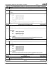
Note: This register configures the Core Logic module to support a 3V Suspend mode. Setting bit 0 causes the SUSP_3V signal to
assert after the appropriate conditions, stopping the system clocks. A delay of 0-15 ms is programmable (bits [7:4]) to allow for
a delay for the clock chip and CPU PLL to stabilize when an event Resumes the system.
A write to the CPU Suspend Command register (F0 Index AEh) with bit 0 written as:
0: Internal SUSP#/SUSPA# handshake occurs. The GX1 module is put into a low-power state, and the system clocks are not
stopped. When a break/resume event occurs, it releases the CPU halt condition.
1: Internal SUSP#/SUSPA# handshake occurs and the SUSP_3V signal is asserted, thus invoking a full system Suspend (both
GX1 module and system clocks are stopped). When a break event occurs, the SUSP_3V signal is de-asserted, the PLL delay
programmed in bits [7:4] are invoked which allows the clock chip and GX1 module PLL to stabilize before de-asserting the
internal SUSP# signal.
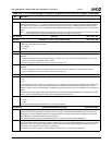
Index BDh-BFh Reserved Reset Value: 00h
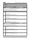
Index C0h-C3h User Defined Device 1 Base Address Register (R/W) Reset Value: 00000000h
31:0 User Defined Device 1 Base Address. This 32-bit register supports power management (Trap and Idle timer resources)
for a PCMCIA slot or some other device in the system. The value in this register is used as the address comparator for the
device trap/timer logic. The device can be memory or I/O mapped (configured in F0 Index CCh).
The Core Logic module cannot snoop addresses on the Fast-PCI bus unless it actually claims the cycle. Therefore, Traps
and Idle timers cannot support power management of devices on the Fast-PCI bus.
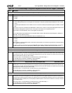
Index C4h-C7h User Defined Device 2 Base Address Register (R/W) Reset Value: 00000000h
31:0 User Defined Device 2 Base Address. This 32-bit register supports power management (Trap and Idle timer resources)
for a PCMCIA slot or some other device in the system. The value in this register is used as the address comparator for the
device trap/timer logic. The device can be memory or I/O mapped (configured in F0 Index CDh).
The Core Logic module cannot snoop addresses on the Fast-PCI bus unless it actually claims the cycle. Therefore, Traps
and Idle timers cannot support power management of devices on the Fast-PCI bus.
Index C8h-CBh User Defined Device 3 Base Address Register (R/W) Reset Value: 00000000h
31:0 User Defined Device 3 Base Address. This 32-bit register supports power management (Trap and Idle timer resources)
for a PCMCIA slot or some other device in the system. The value in this register is used as the address comparator for the
device trap/timer logic. The device can be memory or I/O mapped (configured in F0 Index CEh).
The Core Logic module cannot snoop addresses on the Fast-PCI bus unless the it actually claims the cycle. Therefore,
Traps and Idle timers cannot support power management of devices on the Fast-PCI bus.
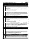
Table 6-29. F0: PCI Header/Bridge Configuration Registers for GPIO and LPC Support (Continued)
Bit Description


