200 AMD Geode™ SC3200 Processor Data Book
Core Logic Module - Bridge, GPIO, and LPC Registers - Function 0
32581C
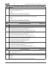
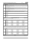
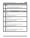
Index 78h-7Bh DOCCS# Base Address Register (R/W) Reset Value: 00000000h
31:0 DiskOnChip Chip Select Base Address. This 32-bit value represents the memory base address used to enable assertion
of DOCCS# (BGU481 ball A9 or N31, see PMR[23] in Table 4-2 on page 70).
This register is used in conjunction with F0 Index 7Ch (DOCCS# Control register).
Index 7Ch-7Fh DOCCS# Control Register (R/W) Reset Value: 00000000h
This register is used in conjunction with F0 Index 78h (DOCCS# Base Address register).
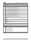
31:27 Reserved. Must be set to 0.
26 DiskOnChip Chip Select Positive Decode (DOCCS#).
0: Disable.
1: Enable.
25 Writes Result in Chip Select. When this bit is set to 1, writes to configured memory address (base address configured in
F0 Index 78h; range configured in bits [18:0]) cause DOCCS# to be asserted.
0: Disable.
1: Enable.
24 Reads Result in Chip Select. When this bit is set to 1, reads from configured memory address (base address configured in
F0 Index 78h; range configured in bits [18:0]) cause DOCCS# to be asserted.
0: Disable.
1: Enable.
23:19 Reserved. Must be set to 0.
18:0 DOCCS# Memory Address Range. This 19-bit mask is used to qualify accesses on which DOCCS# is asserted by mask-
ing the upper 19 bits of the incoming PCI address (AD[31:13]).
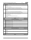
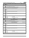
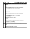
Index 80h Power Management Enable Register 1 (R/W) Reset Value: 00h
7:6 Reserved. Must be set to 0.
5 Codec SDATA_IN SMI. When set to 1, this bit allows an SMI to be generated in response to an AC97 codec producing a
positive edge on SDATA_IN.
0: Disable.
1: Enable.
Top level SMI status is reported at F1BAR0+I/O Offset 00h/02h[0].
Second level SMI status is reported at F0 Index 87h/F7h[2].
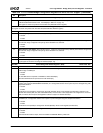
4 Video Speedup. Any video activity, as decoded from the serial connection (PSERIAL) from the GX1 module disables clock
throttling (via internal SUSP#/SUSPA# handshake) for a configurable duration when system is power-managed using CPU
Suspend modulation.
0: Disable.
1: Enable.
The duration of the speedup is configured in the Video Speedup Timer Count Register (F0 Index 8Dh). Detection of an
external VGA access (3Bx, 3Cx, 3Dx and A000h-B7FFh) on the PCI bus is also supported. This configuration is non-stan-
dard, but it does allow the power management routines to support an external VGA chip.
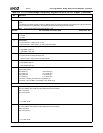
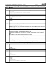
3 IRQ Speedup. Any unmasked IRQ (per I/O Ports 021h/0A1h) or SMI disables clock throttling (via internal SUSP#/SUSPA#
handshake) for a configurable duration when system is power-managed using CPU Suspend modulation.
0: Disable.
1: Enable.
The duration of the speedup is configured in the IRQ Speedup Timer Count Register (F0 Index 8Ch).
2 Traps. Globally enable all power management I/O traps.
0: Disable.
1: Enable.
This excludes the audio I/O traps, which are enabled via F3BAR0+Memory Offset 18h.
Table 6-29. F0: PCI Header/Bridge Configuration Registers for GPIO and LPC Support (Continued)
Bit Description


