


Alpha 21264/EV67 Hardware Reference Manual
Cache and External Interfaces 4–19
System Port
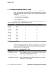
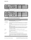
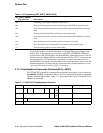
Table 4–9 lists the program values for CSR SYS_FRAME_LD_VECTOR[4:0] that set
the ratio between the forwarded clocks and the frame clock.
4.7.3 21264/EV67-to-System Commands
This section describes the 21264/EV67-to-system commands format and operation. The
command, address, ID, and mask bits are transmitted in four consecutive cycles on
SysAddOut_L[14:0]. The 21264/EV67 sends the command information in one of the
two following modes as selected by the Cbox CSR bit.
• Bank interleave on cache block boundary mode—SYSBUS_FORMAT[0] = 0
• Page hit mode—SYSBUS_FORMAT[0] = 1
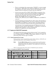
The physical address (PA) bits arrangements for the two modes is shown in Tables 4–10
and 4–11. The purpose of the two modes is to give the system the PA bits that allow it to
select the memory bank and drive the RAS address as soon as possible.
4.7.3.1 Bank Interleave on Cache Block Boundary Mode
Table 4–10 shows the command format for the bank interleave on cache block bound-
ary mode of operation (21264/EV67-to-system).
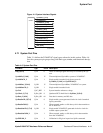
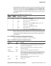
SYS_DDM_RD_RISE_EN[0] Enables the sampling of incoming data on the rising edge of the incoming
forwarded clock. (Always asserted)
SYS_DDMF_ENABLE Enables the falling edge of the system forwarded clock. (Always asserted)
SYS_DDMR_ENABLE Enables the rising edge of the system forwarded clock. (Always asserted)
Table 4–9 Forwarded Clocks and Frame Clock Ratio
Clock Ratio Transfer Mode Value
1
1
These are hexadecimal values.
1:1 All 00
2:1 3.0X, 3.5X, 8.0X 1E
2:1 1.5X, 2.0X, 2.5X 4.0X, 5.0X, 6.0X 7.0X 1F
4:1 8X 15
4:1 1.5X, 4.0X, 5.0X, 6.0X, 7.0X 0B
4:1 3.0X, 3.5X 14
4:1 2.0X, 2.5X 0A
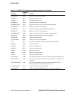
Table 4–10 Bank Interleave on Cache Block Boundary Mode of Operation
SysAddOut_L[14:2] SysAddOut_L[1] SysAddOut_L[0]
Cycle 1 M1 Command[4:0] PA[34:28] PA[36] PA[38]
Table 4–8 Program Values for Data-Sample/Drive CSRs (Continued)
CBOX CSR Description