


Alpha 21264/EV67 Hardware Reference Manual
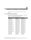
21264/EV67-to-Bcache Pin Interconnections E–3
Dual-Data Rate SSRAMs
E.3 Dual-Data Rate SSRAMs
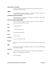
Table E–4 provides the data pin connections between dual-data rate SSRAMs and the
21264/EV67 or the system board. Table E–5 provides the same information for the tag
pins.
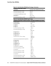
Data and Tag Pin Usage
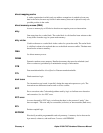
Set from board to 1/2 the 21264/EV67 core voltage CK_L
Set from board to 1/2 the 21264/EV67 core voltage VREF1_H
VREF2_H
Set from board (implementation dependent) ZQ_H
BcTagValid_H DQx
BcTagDirty_H DQx
BcTagShared_H DQx
Unconnected TMS_H
Unconnected TDI_H
Unconnected TCK_H
Unconnected TDC_H
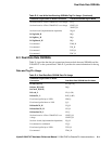
Table E–4 Dual-Data Rate SSRAM Data Pin Usage
21264/EV67 Signal Name or Board
Connection Dual-Data Rate SSRAM Data Pin Name
BcAdd_H[21:4] SA_H[17:0]
BcData_H[33:20]/
BcCheck_H[15:0]
DQx
BcLoad_L LD_L (B1)
BcDataWr_L R/W_L(B2)
From board, pulled up to VDD LBO_L
From board, pulled down to VSS Q_L
BcDataInClk_H CQ_H
BcDataOutClk_H CK_H
BcDataOutClk_L CK_L
Set from board to 1/2 the 21264/EV67 core
voltage
VREF1_H
VREF2_H
Set from board (implementation-dependent) ZQ_H
Unconnected or terminated CQ_L
From board, pulled up to VDD TCK_H
Unconnected TDO_H
Table E–3 Late-Write Non-Bursting SSRAMs Tag Pin Usage (Continued)
21264/EV67 Signal Name or Board Connection Late-Write SSRAM Tag Pin Name