


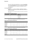
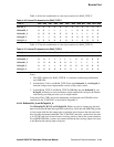
4–48 Cache and External Interfaces
Alpha 21264/EV67 Hardware Reference Manual
Bcache Port
have been programmed for the Bcache clock period, and with satisfactory delay param-
eters for the SSRAM setup/hold Bcache address latch requirements, a Bcache read
command proceeds through the 21264/EV67 Cbox as follows:
1. When the 21264/EV67 clocks out the first address value on the Bcache index pins
with the appropriate Int_Add_BcClk value, the Cbox loads the values of Cbox CSR
BC_LAT_DATA_PATTERN[31:0] and Cbox CSR
BC_LAT_TAG_PATTERN[23:0] into two shift registers, which shift during every
GCLK cycle.
2. The address and control pins are latched into the SSRAMs. During the next cycle,
the SSRAMs provide data and tag information to the 21264/EV67.
3. Using the returning forwarded clocks (BcDataInClk_H[7:0], BcTagInClk_H), the
data/tag information is loaded into the 21264/EV67 clock forwarding queue for the
Bcache.
4. Based on the value of BC_RCV_MUX_PRESET_CNT[1,0] (the unload pointer),
the result of a Bcache write command is loaded into a 21264/EV67 GCLK
(BPHASE) register.
5. The Cbox CSR BC_LAT_DATA_PATTERN[31:0] and
BC_LAT_TAG_PATTERN[23:0] contain the GCLK frequency at which the output
of the clock forward FIFO can be consumed by the processor. This provides GCLK
granularity for the Bcache interface, so that the 21264/EV67 can minimize latency
to the Bcache. When the values based on these Cbox CSRs are shifted down to the
bottom of the shift register, the processor samples the Bcache data and delivers it to
the consumers of load data in the 21264/EV67 functional units.
For example, when a 2.5X-SD SSRAM has a latency of eight GCLK cycles from
BcAdd_H[23:4] to the output of Bcache FIFO, Cbox CSR
BC_LAT_DATA_PATTERN[31:0] is programmed to 948
16
and Cbox CSR
BC_LAT_TAG_PATTERN[23:0] is programmed to 8
16
. The data pattern contains the
placement for four pieces of data and the aggregate rate of the data is 2.5X. In addition,
bit one of the BC_LAT_DATA_PATTERN is placed at a GCLK latency of six GCLK
cycles, which is the minimum latency supported by the 21264/EV67. The
BC_LAT_TAG_PATTERN contains the placement of the tag data to the 21264/EV67.
A shift of one to the left increases the latency of the Bcache transfer to nine GCLK
cycles, and a shift to the right reduces the latency of the Bcache transfer to seven GCLK
cycles.
The Cbox performs isolated tag read transactions in response to system probe com-
mands. In addition, when using burst-mode SSRAMs, the Cbox can combine a separate
tag read transaction with the tail end of a data read transaction, thus optimizing Bcache
bandwidth. A Bcache tag read transaction proceeds exactly like a Bcache data read
transaction, except that only the BC_LAT_TAG PATTERN is used to update the tag
shift register.
4.8.3.2 Bcache Data Write Transactions
During a data write transaction, the 21264/EV67 always writes four pieces of data (64
bytes of data and 8 bytes of ECC) to the Bcache, and always writes the tag array during
the first cycle. Once started, data write operations are never cancelled. Given the appro-