


4–34 Cache and External Interfaces
Alpha 21264/EV67 Hardware Reference Manual
System Port
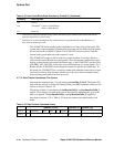
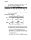
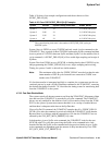
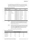
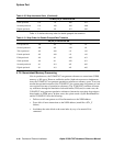
Table 4–27 lists information for the four timing examples. In Table 4–27, note the fol-
lowing:
• SysDc write commands are not affected by the SYSDC_DELAY parameter.
• The SYS_RCV_MUX_PRESET adds delay at the rate of one INT_FWD_CLK at a
time. For example, adding the delay of one bit time to system 1 adds 1.5 GCLK
cycles to the delay and drives the SysDc write command-to-data relationship from
one to two SYSCLKs.
• For write transfers, the 21264/EV67 drivers are enabled on the preceding GCLK
BPHASE, before the start of a write transfer, and disabled on the succeeding GCLK
BPHASE at the end of the write transfer. The write data is enveloped by the 21264/
EV67 drivers to guarantee that every data transfer has the same data valid window.
The four examples described here assume no skew for the 2.0X and 4.0X cases and one
bit time of skew for the 1.5X and 2.5X cases.
For system 1, the distance between SysDc and the first SYSCLK is nine GCLK cycles
but the additional delay of one bit time (1.5 GCLKs) puts the actual delay after perceiv-
ing the SysDc command to 7.5 GCLKS, which misses the 8.5 cycle constraint. There-
fore, the 21264/EV67 drives data two SYSCLKs after receiving the SysDc write
command.
For system 2, the distance between SysDc and the second SYSCLK is eight GCLK
cycles, which also misses the 8.5 cycle constraint, so the 21264/EV67 drives data three
SYSCLK cycles after receiving the SysDc write command (12 cycles).
The other two cases are derived in a similar manner.
4.7.8.4 SysDataInValid_L and SysDataOutValid_L
The SysDataValid signals (SysDataInValid_L and SysDataOutValid_L) are driven by
the system and control the rate of data delivery to and from the 21264/EV67.
SysDataInValid_L
The
SysDataInValid_L signal controls the flow of data into the 21264/EV67, and may
be used to introduce an arbitrary number of cycles between octaword transfers into the
21264/EV67. The rules for using SysDataInValid_L follow:
Table 4–27 Four Timing Examples
System Bit Rate System Framing Clock Ratio
1
1
The system framing clock ratio is the number of INT_FWD_CLK cycles per
SYSCLK cycles.
Write Data
System 1 1.5X 4:1 2 SYSCLKs
System 2 2.0X 2:1 3 SYSCLKs
System 3 2.5X 2:1 2 SYSCLKs
System 4 4X 2:1 2 SYSCLKs