


Alpha 21264/EV67 Hardware Reference Manual
Initialization and Configuration 7–3
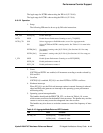
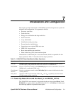
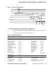
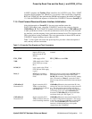
Power-Up Reset Flow and the Reset_L and DCOK_H Pins
Figure 7–1 Power-Up Timing Sequence
7.1.1 Power Sequencing and Reset State for Signal Pins
Power sequencing and avoiding potential failure mechanisms is described in Section
9.3.
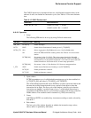
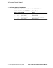
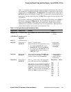
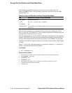
The reset state for the signal pins is listed in Table 7–2.
Table 7–2 Signal Pin Reset State
Signal Reset State Signal Reset State
Bcache
BcAdd_H[23:4] Tristated
BcCheck_H[15:0] Tristated BcTagInClk_H NA (input)
BcData_H[127:0] Tristated BcTagOE_L Tristated
BcDataInClk_H[7:0] NA (input) BcTagOutClk_x Tristated
BcDataOE_L Tristated BcTagParity_H Tristated
BcDataOutClk_x[3:0] Tristated BcTagShared_H Tristated
BcDataWr_L Tristated BcTagValid_H Tristated
BcLoad_L Tristated BcTagWr_L Tristated
BcTag_H[42:20] Tristated BcVref NA
(I_DC_REF)
BcTagDirty_H Tristated
System Interface
IRQ_H[5:0] NA (input) SysDataInClk_H[7:0] NA (input)
SysAddIn_L[14:0] NA (input) SysDataInValid_L NA (input)
SysAddInClk_L NA (input) SysDataOutClk_L[7:0] Tristated
IRQ_H
DCOK_H
state
SromOE_L
internal ClkFwdRst
TestStat_H
external Clks
valid
WAIT_NOMINALWAIT_SETTLE RAMP1 RAMP2 WAIT_ClkFwdRst0 WAIT_BiST
WAIT_ClkFwdRst1
no min no min
End of BiST
BiST Fails BiST Passes
A0
a
B
b
c
f
C
g
d
e
FM-
06
4
86
B.FH
8
A1
RUN
ClkFwdRst_H
Reset_L