


Alpha 21264/EV67 Hardware Reference Manual
Cache and External Interfaces 4–45
Bcache Port
BcTagShared_H
BcTagValid_H
3. The Bcache clock pins (BcDataOutClk
_
x
[3:0] and BcTagOutClk_
x
) clock the
index and data pins at the SSRAMs. These clocks can be delayed from
Int_Data_BcClk from 0 to 2 GCLK phases (half cycles) using Cbox CSR
BC_CPU_CLK_DELAY[1:0].
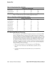
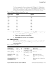
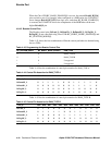
Table 4–37 provides the BC_CPU_CLK_DELAY[1:0] values, which is the delay
from BC_ADDRESS to BC_WRITE_DATA (and BC_CLOCK_OUT) in GCLK
cycles.
In the 21264/EV67 topology, the index pins are loaded by all the SSRAMs, while the
clock and data pins see a limit load. This arrangement requires a relatively large amount
of delay between the index pins and the Bcache clock pins to meet the setup constraints
at the SSRAMs. The 21264/EV67 Cbox CSRs can provide a programmable amount of
delay between the index and clock pins by using Cbox CSRs
BC_CPU_CLK_DELAY[1:0] and BC_CLK_DELAY[1:0].
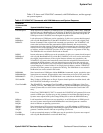
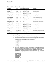
Table 4–38 provides the BC_CLK_DELAY[1:0] values, which is the delay from
BC_WRITE_DATA to BC_CLOCK_OUT, in GCLK phases.
With BC_CPU_CLK_DELAY[1:0] and BC_CLK_DELAY[1:0], a 500-MHz 21264/
EV67 can provide up to 8 ns (3 × 2 + 2) of delay between the index and the outgoing
forwarded clocks. The relative loading difference between the data and the clock is
minimal, so Cbox CSR BC_CLK_DELAY[1:0] alone is sufficient to provide the delay
needed for the setup constraint at the Bcache data register.
4.8.2.1 Setting the Period of the Cache Clock
The free running Bcache clocks are derived from the 21264/EV67 GCLK. The period
of the Bcache clocks is programmed using the following three Cbox CSRs:
1. BC_CLK_LD_VECTOR[15:0]
2. BC_BPHASE_LD_VECTOR[3:0]
Table 4–37 BC_CPU_CLK_DELAY[1:0] Values
BC_CPU_CLK_DELAY[1:0] Value GCLK Cycles of Delay
00
11
22
33
Table 4–38 BC_CLK_DELAY[1:0] Values
BC_CLK_DELAY[1:0] Value GCLK Phases
0 Invalid (turns off BC_CLOCK_OUT)
10
21
32