


4–52 Cache and External Interfaces
Alpha 21264/EV67 Hardware Reference Manual
Bcache Port
When the Cbox CSR BC_BANK_ENABLE[0] is not set, the unused BcAdd_H[23:4]
pins are tied to zero. For example, when configured as a 4MB cache, the 21264/EV67
never changes BcAdd_H[23:22] from logic zero, and when BC_BANK_ENABLE[0]
is asserted, the 21264/EV67 drives the complement of the MSB index on the next
higher BcAdd_H pin.
4.8.4.2 Bcache Control Pins
The Bcache control pins (BcLoad_L, BcDataWr_L, BcDataOE_L, BcTagWr_L,
BcTagOE_L) are controlled using Cbox CSRs BC_BURST_MODE_ENABLE[0] and
BC_PENTIUM_MODE[0].
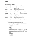
Table 4–43 shows the four combinations of Bcache control pin behavior obtained using
the two CSRs.
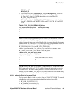
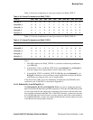
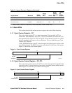
Table 4–44 lists the combination of control pin assertion for
RAM_TYPE A.
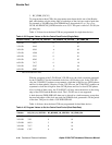
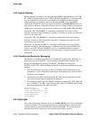
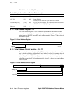
Table 4–45 lists the combination of control pin assertion for RAM_TYPE B.
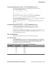
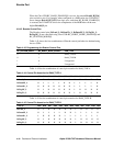
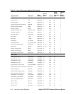
Table 4–43 Programming the Bcache Control Pins
BC_PENTIUM_MODE BC_BURST_MODE_ENABLE RAM_TYPE
0 0 RAM_TYPE A
0 1 RAM_TYPE B
1 0 Unsupported
1 1 Unsupported
Table 4–44 Control Pin Assertion for RAM_TYPE A
TYPE_A NOP RA0 RA1 RA2 RA3 NOP NOP WA0 WA1 WA2 WA3 NOP
BcLoad_L HHHHHHHHH H H H
BcDataOE_L HLLLLHHLL L L H
BcDataWr_L HHHHHHHLL L L H
BcTagOE_L HLHHHHHLH H H H
BcTagWr_L HHHHHHHLH H H H
Table 4–45 Control Pin Assertion for RAM_TYPE B
TYPE_B NOP RA0 RA1 RA2 RA3 NOP NOP WA0 WA1 WA2 WA3 NOP
BcLoad_L HLHHHHHLHHHH
BcDataOE_L HLLLLHHLLLLH
BcDataWr_L LHHHHLLLLLLL
BcTagOE_L HLHHHHHLHHHH
BcTagWr_L HHHHHHHLHHHH