4–54 Cache and External Interfaces
Alpha 21264/EV67 Hardware Reference Manual
Interrupts
4.8.5 Bcache Banking
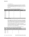
Bcache banking is possible by decoding the index MSB (as determined by Cbox CSR
BC_SIZE[3:0]) and asserting Cbox CSR BC_BANK_ENABLE[0]. To facilitate bank-
ing, the 21264/EV67 provides the complement of the MSB bit in the next higher
unused index bit. For example, when configured as an 8MB cache with banking
enabled, the 21264/EV67 drives the inversion of PA[22] on BcAdd_H[23] for use as a
chip enable in a banked configuration. Because there is no higher index bit available for
16MB caches, this scheme only works for cache sizes of 1MB, 2MB, 4MB, and 8MB.
Setting BC_RD_RD_BUBBLE to 1 introduces one Bcache clock cycle of delay
between consecutive read transactions, regardless of whether or not they are read trans-
actions to the same bank.
Setting BC_WR_WR_BUBBLE to 1 introduces one Bcache clock cycle of delay
between consecutive write transactions, regardless of whether or not they are write
transactions to the same bank.
Setting BC_SJ_BANK_ENABLE to 1 introduces one Bcache clock cycle of delay
between consecutive read transactions to a different bank (based on the MSB of the
index), even if BC_RD_RD_BUBBLE is set to 0. No additional delay is inserted
between consecutive read transactions to the same bank or between consecutive write
transactions.
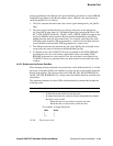
4.8.6 Disabling the Bcache for Debugging
The Bcache is a required component for a 21264/EV67-based system. However, for
debug purposes, the 21264/EV67 can be operated with the Bcache disabled. The
Bcache can be disabled by clearing all of the BC_ENABLE bits in the Cbox
WRITE_MANY CSR. When disabling the Bcache, the following additional steps must
be taken:
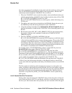
1. The various Bcache control bits in the Cbox WRITE_ONCE chain must be pro-
grammed to a valid combination (normally the same settings that would be used if
the Bcache were enabled).
2. The Bcache must still be initialized (using BC_INIT mode) during the reset PAL
flow, after which the Bcache should be left disabled.
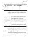
3. Error Detection and Correction should be disabled by clearing DC_DAT_ERR_EN
(bit 7 of the DC_CTL IPR), or the following bits in the Cbox WRITE_ONCE chain
must be programmed to the indicated values:
BC_CLK_DELAY[1:0] = 0x1
BC_CPU_CLK_DELAY[1:0] = 0x1
BC_CPU_LATE_WRITE_NUM[1:0] = 0x1
BC_LATE_WRITE_NUM[2:0] = 0x0
BC_LATE_WRITE_UPPER = 0
DUP_TAG_ENABLE = 0
4.9 Interrupts
The system may request interrupts by way of the IRQ_H[5:0] pins. These six interrupt
sources are identical. They may be asynchronous, are level sensitive, and can be indi-
vidually masked by way of the EIE field of the CM_IER IPR. The system designer
determines how these signals are used and selects their relative priority.


