


4–44 Cache and External Interfaces
Alpha 21264/EV67 Hardware Reference Manual
Bcache Port
4.8.2 Bcache Clocking
For clocking, the Bcache port pins can be divided into three groups.
1. The Bcache index pins (address and control) are referenced to Int_Add_BcClk, an
internal version of the Bcache forwarded clock. The index pins are valid for the
whole period of the Int_Add_BcClk. The index pins are:
BcAdd_H[23:4]
BcDataOE_L
BcDataWr_L
BcLoad_L
BcTagOE_L
BcTagWr_L
2. The data pins, when driven as outputs, are referenced to Int_Data_BcClk, another
internal version of the Bcache forwarded clock. The data pins, when used as inputs,
can be referenced to the incoming Bcache clocks, BcDataInClk_H[7:0] and
BcTagInClk_H. Int_Data_BcClk can be delayed relative to Int_Add_BcClk from
0 to 3 GCLK cycles by using Cbox CSR BC_CPU_CLK_DELAY[1:0]. The data
pins are:
BcCheck_H[15:0]
BcData_H[127:0]
BcTag_H[42:20]
BcTagDirty_H
BcTagParity_H
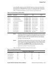
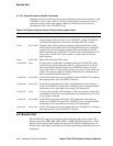
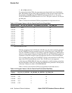
BcDataWr_L O_PP 1 Int_Index_BcClk Bcache data write enable
BcLoad_L O_PP 1 Int_Index_BcClk Bcache burst enable
BcTag_H[42:20] B_DA_PP 23 Int_Data_BcClk ⇒ output
BcTagInClk_H ⇒ input
Bcache tag data
BcTagDirty_H B_DA_PP 1 Int_Data_BcClk ⇒ output
BcTagInClk_H ⇒ input
Bcache tag dirty bit
BcTagInClk_H I_DA 1 NA Tag input data reference clock
BcTagOE_L O_PP 1 Int_Index_BcClk Bcache tag output enable/chip
select
BcTagOutClk_H
BcTagOutClk_L
O_PP 2 NA Bcache tag clock— high and low
versions
BcTagParity_H B_DA_PP 1 Int_Data_BcClk ⇒ output
BcTagInClk_H ⇒ input
Bcache tag parity bit
BcTagShared_H B_DA_PP 1 Int_Data_BcClk ⇒ output
BcTagInClk_H ⇒ input
Bcache tag shared bit
BcTagValid_H B_DA_PP 1 Int_Data_BcClk ⇒ output
BcTagInClk_H ⇒ input
Bcache tag valid bit
BcVref I_DC_REF 1 NA Input reference voltage for tag data
BcTagWr_L O_PP 1 Int_Index_BcClk Bcache data write enable
Table 4–36 Bcache Port Pins (Continued)
Pin Name Type Count Reference Clock Description