


Alpha 21264/EV67 Hardware Reference Manual
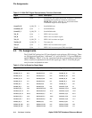
Hardware Interface 3–5
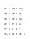
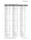
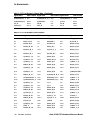
21264/EV67 Signal Names and Functions
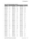
FrameClk_H
FrameClk_L
I_DA_CLK 2 A skew-controlled differential 50% duty cycle copy of the sys-
tem clock. It is used by the 21264/EV67 as a reference, or
framing, clock.
IRQ_H[5:0] I_DA 6 These six interrupt signal lines may be asserted by the system.
The response of the 21264/EV67 is determined by the system
software.
MiscVref I_DC_REF 1 Voltage reference for the miscellaneous pins
(see Table 3–3).
PllBypass_H I_DA 1 When asserted, this signal will cause the two input clocks
(ClkIn_x) to be applied to the 21264/EV67 internal circuits,
instead of the 21264/EV67 global clock (GCLK).
PLL_VDD 3.3 V 1 3.3-V dedicated power supply for the 21264/EV67 PLL.
Reset_L I_DA 1 System reset. This signal protects the 21264/EV67 from dam-
age during initial power-up. It must be asserted until
DCOK_H is asserted. After that, it is deasserted and the
21264/EV67 begins its reset sequence.
SromClk_H O_OD_TP 1 Serial ROM clock. Supplies the clock that causes the SROM to
advance to the next bit. The cycle time for this clock is 256
times the cycle time of the GCLK (internal 21264/EV67
clock).
SromData_H I_DA 1 Serial ROM data. Input data line from the SROM.
SromOE_L O_OD_TP 1 Serial ROM enable. Supplies the output enable to the SROM.
SysAddIn_L[14:0] I_DA 15 Time-multiplexed command/address/ID/Ack from system to
the 21264/EV67.
SysAddInClk_L I_DA 1 Single-ended forwarded clock from system for
SysAddIn_L[14:0] and SysFillValid_L.
SysAddOut_L[14:0] O_OD 15 Time-multiplexed command/address/ID/mask from the 21264/
EV67 to the system bus.
SysAddOutClk_L O_OD 1 Single-ended forwarded clock output for
SysAddOut_L[14:0].
SysCheck_L[7:0] B_DA_OD 8 Quadword ECC check bits for SysData_L[63:0].
SysData_L[63:0] B_DA_OD 64 Data bus for memory and I/O data.
SysDataInClk_H[7:0] I_DA 8 Single-ended system-generated clocks for clock forwarded
input system data.
SysDataInValid_L I_DA 1 When asserted, marks a valid data cycle for data transfers to
the 21264/EV67.
SysDataOutClk_L[7:0] O_OD 8 Single-ended 21264/EV67-generated clocks for clock for-
warded output system data.
SysDataOutValid_L I_DA 1 When asserted, marks a valid data cycle for data transfers from
the 21264/EV67.
SysFillValid_L I_DA 1 When asserted, this bit indicates validation for the cache fill
delivered in the previous system SysDc command.
Table 3–2 21264/EV67 Signal Descriptions (Continued)
Signal Type Count Description