


Alpha 21264/EV67 Hardware Reference Manual
Hardware Interface 3–7
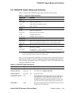
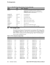
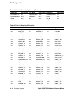
21264/EV67 Signal Names and Functions
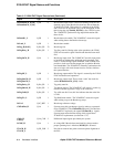
BcVref I_DC_REF 1 Tag data input reference voltage.
SysVref Domain
SysAddIn_L[14:0] I_DA 15 Time-multiplexed SysAddIn, system-to-21264/EV67.
SysAddInClk_L I_DA 1 Single-ended forwarded clock from system for
SysAddIn_L[14:0] and SysFillValid_L.
SysAddOut_L[14:0] O_OD 15 Time-multiplexed SysAddOut, 21264/EV67-to-system.
SysAddOutClk_L O_OD 1 Single-ended forwarded-clock.
SysCheck_L[7:0] B_DA_OD 8 Quadword ECC check bits for SysData_L[63:0].
SysData_L[63:0] B_DA_OD 64 Data bus for memory and I/O data.
SysDataInClk_H[7:0] I_DA 8 Single-ended system-generated clocks for clock forwarded
input system data.
SysDataInValid_L I_DA 1 When asserted, marks a valid data cycle for data transfers to
the 21264/EV67.
SysDataOutClk_L[7:0] O_OD 8 Single-ended 21264/EV67-generated clocks for clock for-
warded output system data.
SysDataOutValid_L I_DA 1 When asserted, marks a valid data cycle for data transfers
from the 21264/EV67.
SysFillValid_L I_DA 1 Validation for fill given in previous SysDC command.
SysVref I_DC_REF 1 System interface reference voltage.
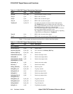
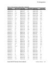
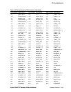
Clocks and PLL
ClkIn_H
ClkIn_L
I_DA_CLK 2 Differential input signals provided by the system.
EV6Clk_H
EV6Clk_L
O_PP_CLK 2 Provides an external test point to measure phase alignment of
the PLL.
FrameClk_H
FrameClk_L
I_DA_CLK 2 A skew-controlled differential 50% duty cycle copy of the
system clock. It is used by the 21264/EV67 as a reference, or
framing, clock.
PLL_VDD 3.3 V 1 3.3-V dedicated power supply for the 21264/EV67 PLL.
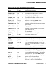
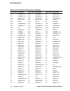
MiscVref Domain
ClkFwdRst_H I_DA 1 Systems assert this synchronous signal to wake up a powered-
down 21264/EV67. The ClkFwdRst_H signal is clocked into
a 21264/EV67 register by the captured FrameClk_x signals.
DCOK_H I_DA 1 dc voltage OK. Must be deasserted until dc voltage reaches
proper operating level. After that, DCOK_H is asserted.
IRQ_H[5:0] I_DA 6 These six interrupt signal lines may be asserted by the system.
MiscVref I_DC_REF 1 Reference voltage for miscellaneous pins.
PllBypass_H I_DA 1 When asserted, this signal will cause the input clocks
(ClkIn_x) to be applied to the 21264/EV67 internal circuits,
instead of the 21264/EV67’s global clock (GCLK).
Table 3–3 21264/EV67 Signal Descriptions by Function (Continued)
Signal Type Count Description