


Alpha 21264/EV67 Hardware Reference Manual
Initialization and Configuration 7–1
7
Initialization and Configuration
This chapter provides information on 21264/EV67-specific microprocessor system ini-
tialization and configuration. It is organized as follows:
• Power-up reset flow
• Fault reset flow
• Energy star certification and sleep mode flow
• Warm reset flow
• Array initialization
• Initialization mode processing
• External interface initialization
• Internal processor register (IPR) reset state
• IEEE 1149.1 test port reset
• Reset state machine state transitions
• Phase-locked loop (PLL) functional description
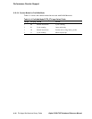
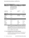
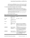
Initialization is controlled by the reset state machine, which is responsible for four
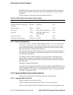
major operations. Table 7–1 describes the four major operations.
7.1 Power-Up Reset Flow and the Reset_L and DCOK_H Pins
The 21264/EV67 reset sequence is triggered using the two input signals Reset_L and
DCOK_H in a sequence that is described in Section 7.1.1. After Reset_L is deasserted,
the following sequence of operations takes place:
Table 7–1 21264/EV67 Reset State Machine Major Operations
Operation Function
Ramp up Sequence the PLL input and output dividers (X
div
and Z
div
) to gradually raise the internal
GCLK frequency and generate time intervals for the PLL to re-establish lock.
BiST/SROM Receive a synchronous transfer on the ClkFwdRst_H pin in order to start built-in self-test and
SROM load at a predictable GCLK cycle.
Clock forward
interface
Receive a synchronous transfer on the ClkFwdRst_H pin in order to initialize the clock for-
warding interface.
Ramp down Sequence the PLL input and output dividers (X
div
and Z
div
) to gradually lower the internal
GCLK frequency during sleep mode.