


Alpha 21264/EV67 Hardware Reference Manual
Privileged Architecture Library Code 6–15
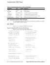
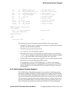
Translation Buffer (TB) Fill Flows
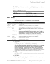
hw_mtprp4, <EV6__DTB_PTE0 ! ^x44> ; (0,4,2,6) (0L) write pte0
hw_mtprp4, <EV6__DTB_PTE1 ! ^x22> ; (3,7,1,5) (1L) write pte1
ASSUME <tb_mb_en + pte_eco> ne 2
.if ne pte_eco
bne p7, trap__dtbm_single_mb ; branch for mb
hw_ret (p23) ; return
trap__dtbm_single_mb:
mb
hw_ret(p23) ; return
.iff
hw_ret(p23) ; return
; (assumes tb_mb_en on multi-processors)
.endc
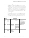
The following list presents information about the single-miss DTB code example:
• In Figure 6–5, where (x,y) or (y) appear in the comments, x specifies the scoreboard
bits and y specifies the Ebox subcluster.
• r4 −r7 and r20 − r23 are PALshadow registers.
• PALshadow r22 contains a flag that indicates whether the native code is running
“1−to−1”, that is, running in a mode where the physical address should be mapped
1−to−1 to the virtual address, rather than being taken from a page table.
• IPR scoreboard bits [3:0] are used to order the restarted load or store instructions
for the DTB write transactions.
• MM_STAT and VA will not be overwritten if the LD_VPTE instruction misses the
DTB. There is no issue order constraint.
• The code is written to prevent a later execution of the DTB fill instruction from
being issued before a previous execution and corrupting the previous write to the
TB registers. The correct sequence of executions is accomplished by placing code
dependencies on scoreboard bits [7:4] in the path of the successive writers. This
prevents the successive writers from being issued before the previous writers are
retired.
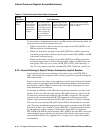
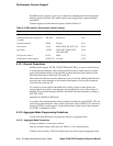
• When I_CTL[TB_MB_EN] = 1, the issue of MTPR DTB_PTE0 triggers, in hard-
ware, a lightweight memory barrier (TB-MB). The lightweight memory barrier
enforces read-ordering of store instructions from another processor (I) to this pro-
cessor’s (J) page table and this processor’s virtual memory area such that if this
processor sees the write to the PTE from (I) it will see the new data.
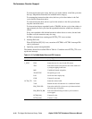
Processor I Processor J
Wr Data LD/ST
MB <tb miss>
Wr PTE LD-PTE, write TB
LD/ST