


Alpha 21264/EV67 Hardware Reference Manual
Initialization and Configuration 7–19
Phase-Lock Loop (PLL) Functional Description
7.11 Phase-Lock Loop (PLL) Functional Description
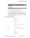
The PLL multiplies the clock frequency of a differential input reference clock and
aligns the phase of its output to that differential input clock. Thus, the 21264/EV67 can
communicate synchronously on clock boundaries with clock periods that are defined by
the system.
7.11.1 Differential Reference Clocks
A skew-controlled, ac-coupled differential clock is provided to the PLL by way of
ClkIn_x . ClkIn_x are input signals to a differential amplifier. The frequency of
ClkIn_x can range from 80 MHz to 200 MHz. ClkIn_x can be sourced by a variety of
components that include PECL fanout parts or system PLLs. ClkIn_x are also the pri-
mary clock source for the 21264/EV67 when in PLL bypass mode.
7.11.2 PLL Output Clocks
The following sections summarize the PLL output clocks.
7.11.2.1 GCLK
The PLL provides an output clock, GCLK, with a frequency that can range from 400
MHz to 833.3 MHz under full-speed conditions. GCLK is the nominal onchip clock
that is distributed to the entire 21264/EV67 chip.
7.11.2.2 Differential 21264/EV67 Clocks
The EV6Clk_x output pads provide an external test point to measure the PLL phase
alignment. They do not provide a clock source. EV6Clk_x are square-wave signals
that drive rail-to-rail continually from 0 to 2.1 volts.
7.11.2.3 Nominal Operating Frequency
Under normal operating conditions, the frequency of the PLL output clock, GCLK, is a
simple function of the Y
div
divider value.
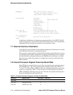
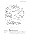
DOWN2 Triggered by duration counter reaching 8205 cycles, the PLL ramps GCLK frequency
down by the first divider ratio (X
div
and Z
div
equal 2 and 4, respectively). This has the
effect of halving the GCLK frequency. The duration counter is set to 4108 cycles.
DOWN3 Triggered by duration counter reaching 4108 cycles, the PLL ramps frequency down by
the second divider ratio (X
div
and Z
div
equal 16 and 32, respectively). This has the
effect of reducing the frequency by a factor of 16 (of the original frequency). The inter-
nal counter is set to 264 cycles.
WAIT_INTERRUPT Triggered by duration counter reaching 264 cycles, the 21264/EV67 waits for either an
unmasked clock interrupt or unmasked device interrupt from system. The interrupts are
wired to the interrupt request and enable internal registers. When an enabled interrupt
occurs, the PLL ramps back to full frequency. Subsequent to that, the built-in self-init
(BiSI) initializes arrayed structures. The SROM is not reloaded; instead, the 21264/
EV67 begins fetching code from the SYSTEM.
Table 7–11 21264/EV67 Reset State Machine State Descriptions (Continued)
State Name Description