


4–30 Cache and External Interfaces
Alpha 21264/EV67 Hardware Reference Manual
System Port
The ChangeToDirtySuccess and ChangeToDirtyFail commands cannot be issued in the
shadow of SysDc cache fill commands (ReadDataError, ReadData, ReadDataDirty,
ReadDataShared, and ReadDataShared/Dirty). Each cache fill command allocates eight
cycles on the SysData bus. Systems are required to ensure that any future SysDc com-
mands do not cause conflicts with those eight SysData bus cycles. In addition, the sys-
tem must not issue ChangeToDirtySuccess or ChangeToDirtyFail commands in the six
SysAddrIn cycles after any of the ReadDatax commands because doing so will over-
load internal MAF resources in the 21264/EV67.
Because of an internal 21264/EV67 constraint, a minimum memory latency of
4 × BCACHE_CLK_PERIOD is imposed. This latency is measured from A3 of the out-
going command (the last cycle) to the delivery of the SysDc command to the processor.
4.7.8 Data Movement In and Out of the 21264/EV67
There are two modes of operation for data movement in and out of the 21264/EV67:
fast mode and fast mode disable. The data movement mode is selected using Cbox CSR
FAST_MODE_DISABLE[0]. Fast data mode allows movement of data from the
21264/EV67 to bypass protocol and achieve the lowest possible latency for probe’s
data, write victim data, and I/O write data. Rules and conditions for the two modes are
listed and described in Sections 4.7.8.2 and 4.7.8.3. Before discussing data movement
operation, 21264/EV67 clock basics are described in Section 4.7.8.1.
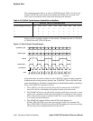
4.7.8.1 21264/EV67 Clock Basics
The 21264/EV67 uses a clock forwarding technique to achieve very high bandwidth on
its pin interfaces. The clock forwarding technique has three main principles:
1. Local point-to-point transfers can be made safely, and at very high bandwidth, if the
sender can provide the receiver with a forward clock (FWD_CLK) to latch the
transmitted data at the receiver.
–The SysAddOutClk_L and SysDataOutClk_L[7:0] pins provide the forward-
ing clocks for transfers out of the 21264/EV67.
–The SysAddInClk_L and SysDataInClk_H[7:0] pins provide the forwarding
clocks for transfers into the 21264/EV67.
2. If only one state element was used to capture the transmitted data, and the skew
between the two clock systems was greater then the bit-rate of the transfer, the data
valid time of the transmitted data would not be sufficient to safely transfer the
latched data into the receivers clock domain. In order to avoid this problem, the
receiver provides a queue that is manipulated in the transmitter’s time domain.
Using this queue, the data valid window of the transmitted data is extended (to an
arbitrary size based on the queue size), and the transfer to the receiver’s clock
domain can be safely made by delaying the unloading of this queue element beyond
the skew between the two clock domains. The internal clock that unloads this queue
is labelled INT_FWD_CLK. INT_FWD_CLK is timed at both the rising and fall-
ing edges of the external clock, thus appearing to run at twice the external clock’s
frequency.
3. The first two points provide the steady state basis for clock forwarded transfers;
however, both the sender and receiver must be correctly initialized to enable coher-
ent and predictable transfers. This clock initialization is performed during system
initialization using the ClkFwdRst_H and FrameClk_H signals.