


5–26 Internal Processor Registers
Alpha 21264/EV67 Hardware Reference Manual
Mbox IPRs
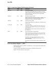
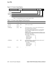
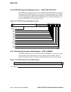
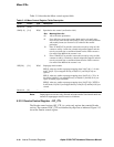
5.3.2 DTB PTE Array Write Registers 0 and 1 – DTB_PTE0, DTB_PTE1
The DTB PTE array write registers 0 and 1 (DTB_PTE0 and DTB_PTE1) are registers
through which the DTB PTE arrays are written. The entries to be written are chosen by
a round-robin allocation scheme. Write transactions to the DTB_PTE registers, when
retired, result in both the DTB_TAG and DTB_PTE arrays being written. Figure 5–27
shows the DTB PTE array write registers 0 and 1.
Figure 5–27 DTB PTE Array Write Registers 0 and 1
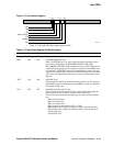
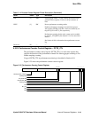
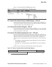
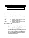
5.3.3 DTB Alternate Processor Mode Register – DTB_ALTMODE
The DTB alternate processor mode register (DTB_ALTMODE) is a write-only register
whose contents specify the alternate processor mode used by some HW_LD and
HW_ST instructions. Figure 5–28 shows the DTB alternate processor mode register.
Figure 5–28 DTB Alternate Processor Mode Register
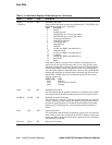
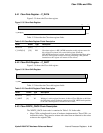
6362 98716 615 514 413 332 12 231 11 110 0
PA[43:13]
UWE
SWE
EWE
KWE
URE
SRE
ERE
KRE
GH[1:0]
ASM
FOW
FOR
LK
99
-
0036
A
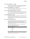
63 210
ALT_MODE[1:0]
LK
99
-
003
7A