


4–46 Cache and External Interfaces
Alpha 21264/EV67 Hardware Reference Manual
Bcache Port
3. BC_FDBK_EN[7:0]
To program these three CSRs, the programmer must know the bit-rate of the Bcache
data, and whether only the rising edge or both edges of the clock are used to latch data.
For example, a 200-MHz late-write SSRAM has a data period of 5 ns. For a 2-ns
GCLK, the READCLK_RATIO must be set to 2.5X. This part is called a 2.5X SD (sin-
gle-data part).
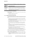
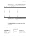
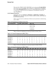
Table 4–39 shows how the three CSRs are programmed for single-data devices.
With the exception of the 2.5X-SD and 3.5X-SD cases, the clock waveform generated
by the 21264/EV67 for the forwarded clocks has a 50-50 duty cycle. In the 2.5X-SD
case, the 21264/EV67 produces an asymmetric clock that is high for two GCLK phases
and low for three phases. Likewise, for the 3.5X-SD case, the 21264/EV67 produces an
asymmetric clock that is high for three GCLK phases and low for four GCLK phases.
Also, for both of these cases, the 21264/EV67 will only start transactions on the rising
edge of the GCLK and the Bcache clock. The 1.5X-SD case is not supported.
A dual-data rate (DDR) SSRAM’s data rate is derived in a similar manner, except that
because both edges of the clock are used, the SSRAM clock generated is 2X the period
of the data. This part is called a 2.5X DDR SSRAM.
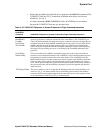
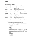
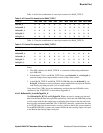
Table 4–40 shows how the three CSRs are programmed for dual-data devices.
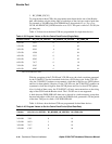
Table 4–39 Program Values to Set the Cache Clock Period (Single-Data)
Bcache Transfer BC_CLK_LD_VECTOR
1
1
These are hexadecimal values.
BC_BPHASE_LD_VECTOR
1
BC_FDBK_EN
1
2.0X-SD 5555 0 01
2.5X-SD 94A5 3 02
3.0X-SD 9249 A 02
3.5X-SD 4C99 C 04
4.0X-SD 3333 0 01
5.0X-SD 8C63 5 02
6.0X-SD 71C7 0 10
7.0X-SD C387 A 04
8.0X-SD 0F0F 0 01
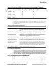
Table 4–40 Program Values to Set the Cache Clock Period (Dual-Data Rate)
Bcache
Transfer BC_CLK_LD_VECTOR
1
BC_BPHASE_LD_VECTOR
1
BC_FDBK_EN
1
1.5X-DD 9249 A 02
2.0X-DD 3333 0 01
2.5X-DD 8C63 5 02
3.0X-DD 71C7 0 10
3.5X-DD C387 A 04