


E–2 21264/EV67-to-Bcache Pin Interconnections
Alpha 21264/EV67 Hardware Reference Manual
Late-Write Non-Bursting SSRAMs
E.2 Late-Write Non-Bursting SSRAMs
Table E–2 provides the data pin connections between late-write non-bursting SSRAMs
and the 21264/EV67 or the system board. Table E–3 provides the same information for
the tag pins.
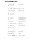
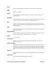
Data Pin Usage
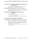
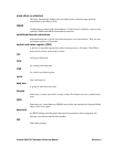
Tag Pin Usage
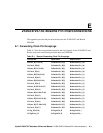
Unused Bcache tag pins should be pulled to ground through a 200-ohm resistor.
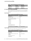
BcTagShared_H BcTagInClk_H BcTagOutClk_x
BcTagDirty_H BcTagInClk_H BcTagOutClk_x
BcTagValid_H BcTagInClk_H BcTagOutClk_x
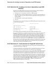
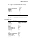
Table E–2 Late-Write Non-Bursting SSRAMs Data Pin Usage
21264/EV67 Signal Name or Board Connection Late-Write SSRAM Data Pin Name
BcAdd_H[21:4] SA_H[17:0]
BcDataOutClk_H[3:0] CK_H
Set from board to 1/2 the 21264/EV67 core voltage CK_L
BcData_H[127:0]/BcCheck_H[15:0] DQx
BcDataWr_L SW_L
Unconnected Tck_H
Unconnected Tdo_H
Unconnected Tms_H
Unconnected Tdi_H
From board, pull down to VSS G_L
From board, pull down to VSS SBx_L
From board, pull down to VSS or BcDataOE_L SS_L (Vendor dependent)
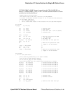
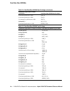
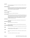
Table E–3 Late-Write Non-Bursting SSRAMs Tag Pin Usage
21264/EV67 Signal Name or Board Connection Late-Write SSRAM Tag Pin Name
BcAdd_H[22:6] SA_H[16:0]
BcTag_H[42:20] DQx
BcTagOE_L or from board, pull down to VSS SS_L (Vendor dependent)
BcTagWr_L SW_L
From board, pull down to VSS SBx_L
BcTagOutClk_H CK_H
Table E–1 Bcache Forwarding Clock Pin Groupings (Continued)
Pad and Pin Input Clock Output Clocks