


Intel
®
820E Chipset
R
Design Guide 143
A designer using components other than those listed previously must evaluate additional combinations of
driver and receiver.
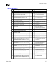
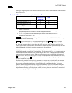
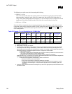
Table 51. AGTL+ Parameters for Example Calculations
1,2
IC Parameters Pentium
®
III
Processor Core at
133 MHz Bus
Intel
®
82820
MCH
Notes
Clock-to-output maximum (T
CO_MAX
) 2.7 3.6 4
Clock-to-output minimum (T
CO_MIN
) -0.1 0.5 4
Setup time (T
SU_MIN
) 1.2 2.27 3,4
Hold time (T
HOLD
) 0.8 0.28 4
NOTES:
1. All times in nanoseconds.
2.
Numbers in table are for reference only. These timing parameters are subject to change. Please check the
appropriate component documentation for the valid timing parameter values.
3. T
SU_MIN
= 1.9 ns assumes the Intel 82820 MCH sees a minimum edge rate equal to 0.3 V/ns.
4. The Pentium III processor substrate’s nominal impedance is set to 65
Ω ± 15%. Future Pentium III processor
substrates may be set at 60
Ω ± 15%.
Table 51 lists the AGTL+ component timings of the processors and Intel 82820 MCH defined at the pins.
These timings are for reference only.
Table 52 gives an example AGTL+ initial maximum flight time and Table 53 contains an example
minimum flight time calculation for a 133 MHz, 2-way Pentium
III processor/Intel 820E chipset system
bus. Note that assumed values for clock skew and clock jitter were used. Clock skew and clock jitter
values depend on the clock components and distribution method chosen for a particular design and must
be budgeted into the initial timing equations as appropriate for each design.
Intel highly recommends adding margin, as shown in the M
ADJ
column, to offset the degradation caused
by SSO push-out and other multi-bit switching effects. The Recommended T
FLT_MAX
column contains the
recommended maximum flight time after incorporating the M
ADJ
value. If the edge rate, ringback, and
monotonicity requirements are not met, flight time correction must first be performed as documented in
the
Intel
®
Pentium
®
II Processor Developer’s Manual, with the additional requirements noted in Section
3.5. The commonly used “textbook” equations used to calculate the expected signal propagation rate of a
board are included in Section 3.2.
Simulation and control of baseboard design parameters can ensure that the signal quality and maximum
and minimum flight times are met. Baseboard propagation speed is highly dependent on the transmission
line geometry configuration (stripline vs. microstrip), dielectric constant, and loading. This layout
guideline includes high-speed baseboard design practices that may improve the amount of timing and
signal quality margin. The magnitude of M
ADJ
is highly dependent on the baseboard design
implementation (stack-up, decoupling, layout, routing, reference planes, etc.) and must be characterized
and budgeted appropriately for each design.