Intel
®
820E Chipset
R
Design Guide 157
3.4.3.2. Reference Planes and PCB Stack-Up
It is strongly recommended that baseboard stack-up be arranged such that AGTL+ signals are
referenced to a ground (V
SS
) plane, and that the AGTL+ signals do not traverse multiple signal layers.
Deviating from either guideline can create discontinuities in the signal’s return path, that can lead to large
SSO effects that degrade the timing and noise margin. Designing an AGTL+ platform incorporating
discontinuities will subject the platform to a risk that is highly unpredictable in pre-layout simulation.
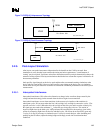
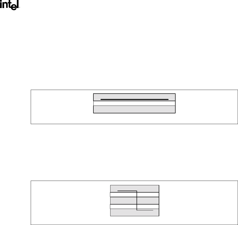
The following figure shows the ideal case, where a particular signal is routed entirely within the same
signal layer, with a ground layer as the single reference plane.
Figure 79. One Signal Layer and One Reference Plane
Ground Plane
Signal Layer A
1lay_1ref-plane
When it is not possible to route the entire AGTL+ signal on a single V
SS
referenced layer, there are
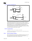
methods of reducing the effects of layer switches. The best alternative is to allow the signals to change
layers while staying referenced to the same plane (see Figure 80). Figures 81 through 83 show other
methods of minimizing layer switch discontinuities, but they may be less effective than the following
figure. In this case, the signal still references the same type of reference plane (i.e., ground). In such a
case, it is important to stitch (i.e., connect) the two ground planes together with vias in the vicinity of the
signal transition via.
Figure 80. Layer Switch with One Reference Plane
lay_sw_1refplane
Signal Layer A
Signal Layer B
Ground Plane


