


Intel
®
820E Chipset
R
166 Design Guide
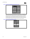
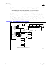
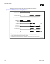
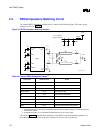
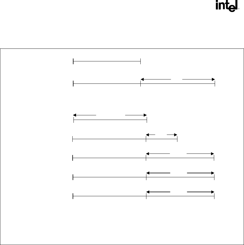
The following figure shows the Intel 820E chipset clock length routing guidelines.
Figure 87. Intel
®
820E Chipset Clock Routing Guidelines
1,2
Note:
1. Tie 3V66 clock for MCH to 3V66 clock for AGP connector, to eliminate pin-to-pin skew.
2. These calculations are based on 150-ps/in trace velocity.
3. TBD value derived from PCI Revision 2.2 Specification, which allows for max. ±2-ns clock skew.
CPUCLK to MCH
Y
CPUCLK to SC242
Note: Tie CPUCLK for the MCH to CPUCLK to the SC242, to eliminate pin-to-pin skew.
±0"
Y
5.3"
3V66 clock for
MCH and ICH
±0"
4"Z
PCI clock for ICH
±0"
4"Z
PCI clock for on-board
devices (excluding ICH)
±TBD
3
4"Z
3V66 clock for
AGP slot
Z
PCI clock for
PCI slots
±TBD
3
1.5"Z
820_clk_route