Intel
®
820E Chipset
R
Design Guide 195
Appendix A: Reference Design
Schematics (Uniprocessor)
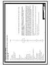
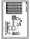
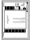
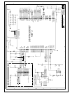
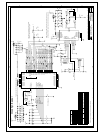
This chapter provides the schematic diagrams for the Reference Board Uniprocessor design.
Reference Design Feature Set
• Intel 820E chipset
Memory controller hub (MCH)
I/O controller hub (ICH2)
FWH Flash BIOS
• Support for Coppermine FC-PGA processors
100 MHz and 133 MHz system bus frequency
Debug port
• IOAPIC integrated into ICH2
• Direct RDRAM memory interface
300 MHz, 356 MHz, and 400 MHz Direct RDRAM support
2 RIMM sockets
• 5 PCI add-in slots
Via 5 REQ/GNT pairs (ICH2 supports 6 REQ#/GNT# pairs.)
Added 4 PCI interrupts (total of 8)
• AGP universal connector
3.3 V: 1×, 2× signaling
1.5 V: 1×, 2×, 4× signaling
• 2 IDE connectors with Ultra ATA/100/66/33, BMIDE, PIO support
• ICH2 2 USB controllers (total of 4 ports)
• ATX power connector
• LPC Ultra I/O
Floppy disk controller
1 parallel port, 1 serial port
Keyboard controller
• Communications networking riser (CNR)
Support for up to 6-channel audio
• WfM support
• Integrated system management
SMBus slave interface access via SMLink
• Integrated power management
ACPI Rev. 1.0 compliant
APM Rev. 1.2 compliant
• Integrated LAN controller
• VRM 8.4-compliant voltage regulator
• Four-layer design


