Intel
®
820E Chipset
R
Design Guide 175
4.9. DRCG Frequency Selection and the DRCG+
4.9.1. DRCG Frequency Selection Table and Jitter Specification
To provide additional flexibility in board design, Intel has enabled a variation of the DRCG, called the
DRCG+. The device has the same specifications, pinout, and form-factor mentioned in the document for
the existing DRCG device. Two modifications were made to the DRCG+.
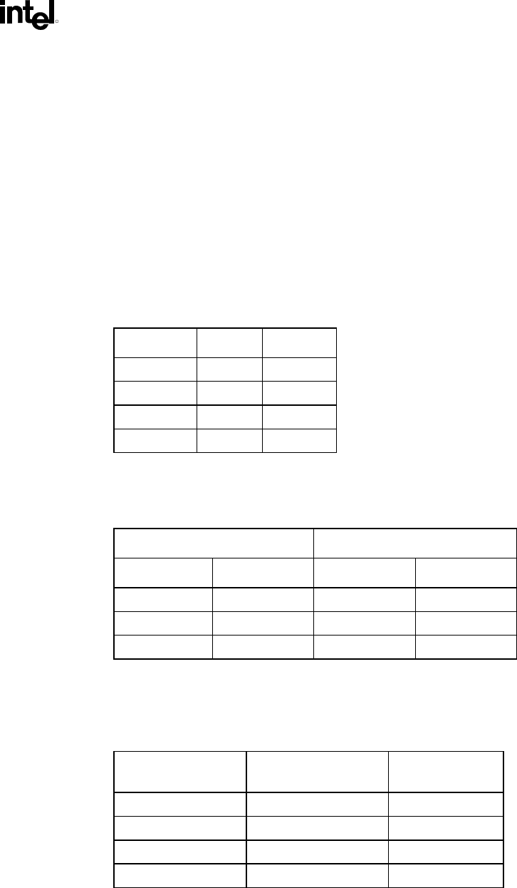
1. The DRCG+ Mult[0:1] select table was changed to modify two of the multiplier ratios. The DRCG+
will support 133/356 MHz using a 66 MHz DRCG+ input clock and a 16/3 multiplier. An additional
9/2 multiplier allows 133/300 MHz (not supported by the Intel 820E chipset). Support for the 300
MHz and 400 MHz memory bus is unchanged. The following table lists the DRCG ratios.
Mult[0:1] DRCG DRCG+
0:0 4:1 9:2
0:1 6:1 6:1
1:0 8:3 16:3
1:1 8:1 8:1
2. The Intel 820E chipset supports the following ratios and can be supported by the DRCG and DRCG+
or derivative devices. Contact your DRCG vendor for information on DRCG, DRCG+, and derivative
products.
100 MHz Host Bus 133 MHz Host Bus
Frequency Multiplier Frequency Multiplier
100 / 300 6:1 133 / 266 4:1
100 / 400 8:1 133 / 356 16:3
133 / 400 6:1
3. The jitter timing specifications were expanded to encompass both the component specification (for
DRCG or derivative products) and the channel specification. Follow the component specification
when measuring jitter at the DRCG output resistor. Follow the channel jitter guidelines when
measuring jitter at the MCH or at the termination for CFM/CFM# on the RDRAM interface.
Output Frequency
(MHz)
Component Jitter
Specification
Channel Jitter
Guidelines
400 50 ps 100 ps
356 60 ps 110 ps
300 70 ps 120 ps
266 80 ps 130 ps


