


Intel
®
820E Chipset
R
Design Guide 67
Note: The motherboard provides 3.3 V to the V
CC
pins of the AGP connector. If the graphics controller needs a
lower voltage, then the add-in card must regulate the 3.3 V V
CC
voltage to the controller’s requirements.
The graphics controller may only power AGP I/O buffers with the V
DDQ
power pins.
The TYPEDET# signal indicates whether the AGP 2.0 interface operates at 1.5 V or 3.3 V. If
TYPEDET# is floating (i.e., no connect) on an AGP add-in card, the interface is 3.3 V. If TYPEDET# is
shorted to ground, the interface is 1.5 V.
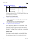
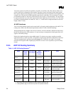
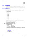
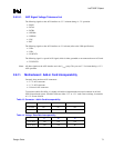
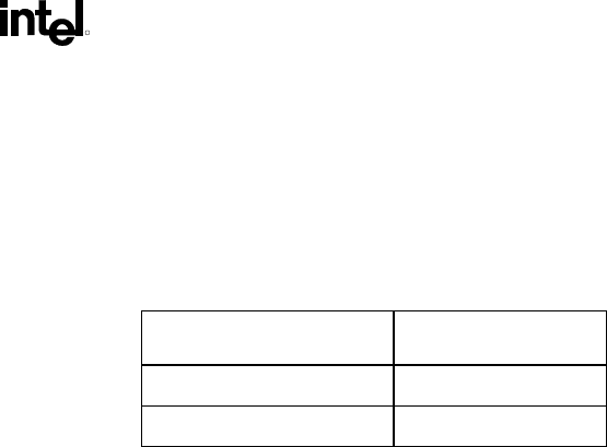
Table 12. TYPDET#/V
DDQ
Relationship
TYPEDET# (on Add-in Card) V
DDQ
(Supplied by MB)
GND 1.5 V
N/C 3.3 V
As a result of this requirement, the motherboard must provide a flexible voltage regulator. This regulator
must supply the appropriate voltage to the V
DDQ
pins on the AGP connector. For specific design
recommendations, refer to the schematics in Appendix A: Reference Design Schematics (Uniprocessor).
V
DDQ
generation and AGP V
REF
generation must be considered together. Before developing V
DDQ
generation circuitry, refer to the AGP 2.0 Interface Specification.
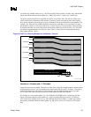
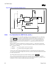
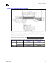
Figure 38 demonstrates one way to design the V
DDQ
voltage regulator. This regulator is a linear regulator
with an external, low-R
DS-ON
FET. The source of the FET is connected to 3.3 V. This regulator will
convert 3.3 V to 1.5 V or pass 3.3 V, depending on the state of TYPEDET#. If a linear regulator is used,
it must draw power from 3.3 V (not 5 V) to control thermals. (i.e., 5 V regulated down to 1.5 V with a
linear regulator will dissipate approximately 7 W at 2 A.) Because it must draw power from 3.3 V and, in
some situations, must simply pass that 3.3 V to V
DDQ
(when a 3.3 V add-in card is placed in the system),
the regulator must use a low-R
DS-ON
FET.
AGP 1.0 modified V
DDQ
3.3
MIN
to 3.1 V. When an ATX power supply is used, the 3.3 V
MIN
is 3.168 V.
Therefore, 68 mV of drop is allowed across the FET at 2 A. This corresponds to an FET with an R
DS-ON
of 34 mW.
How does the regulator switch? The feedback resistor divider is set to 1.5 V. When a 1.5 V card is
placed in the system, the transistor is off and the regulator regulates to 1.5 V. When a 3.3 V card is
placed in the system, the transistor is on and the feedback is pulled to ground. When this happens, the
regulator drives the gate of the FET to nearly 12 V. This turns on the FET and passes
3.3 V – 2 A × R
DS-ON
to V
DDQ
.