Intel
®
820E Chipset
R
Design Guide 69
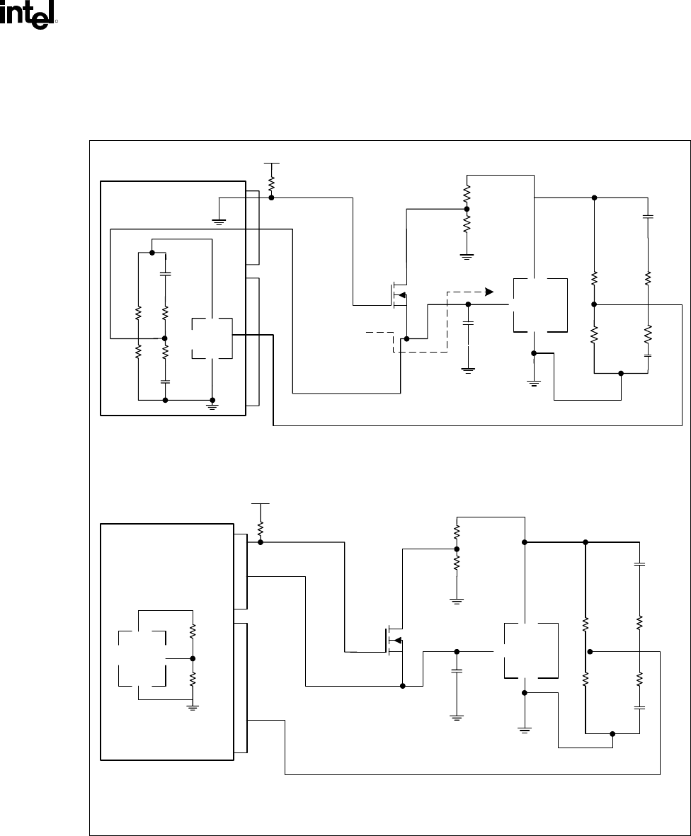
During a 3.3 V AGP 2.0 operation, V
REF
must be 0.4 V
DDQ
. However, during a 1.5 V AGP 2.0 operation,
V
REF
must be 0.5 V
DDQ
. This requires a flexible voltage divider for V
REF
. Various methods of
accomplishing this exist, such as the example in the following figure.
Figure 39. AGP 2.0 V
REF
Generation and Distribution
AGP
device
1.5-V AGP Card
VDDQ
GND
R9
300
Ω
1%
R11
200
Ω
1%
C10
0.1 µF
VDDQ
REF
GND
GMCH
C8
500 pF
REF
U6
MOSFET
R7
1 k
Ω
+12 V
TYPEDET#
VrefCG
VrefGC
VDDQ
Notes:
1. The resistor dividers should be placed near the GMCH. The AGPREF signal must be 5 mils wide and routed 10 mils from adjacent signals.
2. R7 is the same resistor as R1 in the figure AGP VDDQ Generation Example Circuit.
R6
1 k
Ω
R5
82
Ω
R2
1 k
Ω
R4
82
Ω
C9
500 pF
(Note 2)
C8
500 pF
AGP
device
3.3-V AGP Card
VDDQ
GND
C10
0.1 uF
VDDQ
REF
GND
GMCH
R6
1 k
Ω
R2
1 k
Ω
R5
82
Ω
R4
82
Ω
REF
U6
MOSFET
+12 V
TYPEDET#
VrefCG
VrefGC
VDDQ
C9
500 pF
R9
300
Ω
1%
R7
1 k
Ω
(Note 2)
R11
200
Ω
1%
Notes:
1. The resistor dividers should be placed near the GMCH. The AGPREF signal must be 5 mils wide and routed 25 mils from adjacent signals.
2. R7 is the same resistor as R1 in the figure AGP VDDQ Generation Example Circuit.
AGP2_Vref_gen-dist
Place C10 close to MCH.
Place C10 close to MCH.
The flexible V
REF
divider shown in the preceding figure uses an FET switch to switch between the locally
generated V
REF
(for 3.3 V add-in cards) and the source-generated V
REF
(for 1.5 V add-in cards).
Use of the source-generated V
REF
at the receiver is optional and is a product implementation issue
beyond the scope of this document.


