Intel
®
820E Chipset
R
168 Design Guide
4.2. Component Placement and Interconnection Layout
Requirements
The layout requirements for each interconnection are explained in detail in the following sections:
• Crystal to CK133
• CK133 to DRCG
• MCH to DRCG
• DRCG to RDRAM channel
4.2.1. 14.318 MHz Crystal to CK133
The distance between the crystal and the CK133 should be minimized. The maximum trace length is
500 mils.
4.2.2. CK133 to DRCG
• Processor _div2
• VddIR – Used as a reference for 2.5 V signaling
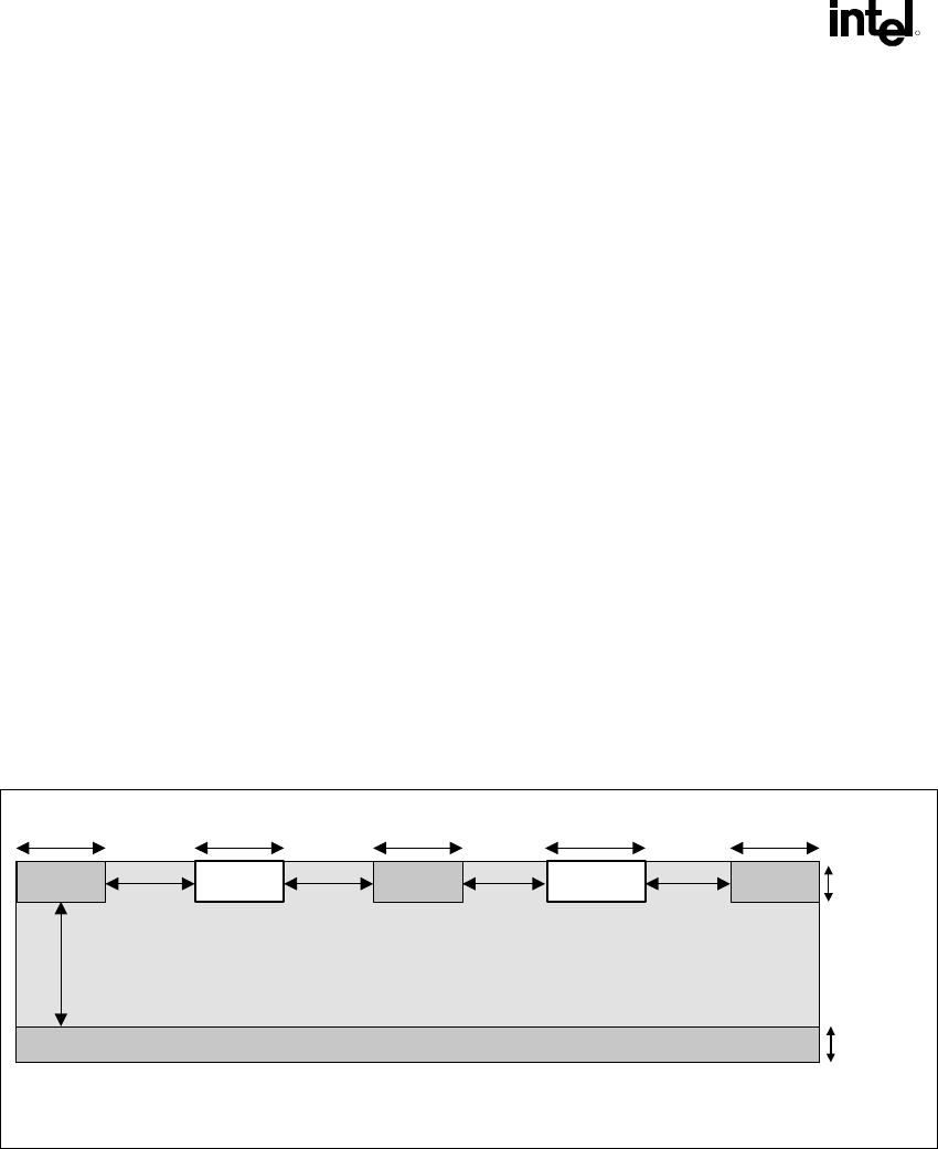
Figure 88. CK133-to-DRCG Routing Diagram
Ground
Ground/Power Plane
6 mils
4.5 mils
1.4 mils
1.4 mils
6 mils
VddiR
6 mils
6 mils
Ground
6 mils
6 mils
CPU_div2
6 mils
6 mils
Ground
6 mils
ck133_drcg_route
VddIR and CPU_div2 must be routed as shown in Figure 88. Note that the VddIR pin can be connected
directly to 2.5 V near the DRCG if the 2.5 V plane extends near the DRCG. However, if a 2.5 V trace
must be used, it should originate at the CK133 and be routed as shown.


