Intel
®
820E Chipset
R
Design Guide 181
5.1.7. Testing Board Impedance
The Intel Printed Circuit Board (PCB) Test Methodology document (order# 298179-001) should be used
to ensure boards are within the 28
Ω +/- 10% requirement. This document can be found at
http://developer.intel.com
.
5.1.8. Board Impedance/Stack-up Summary
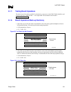
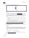
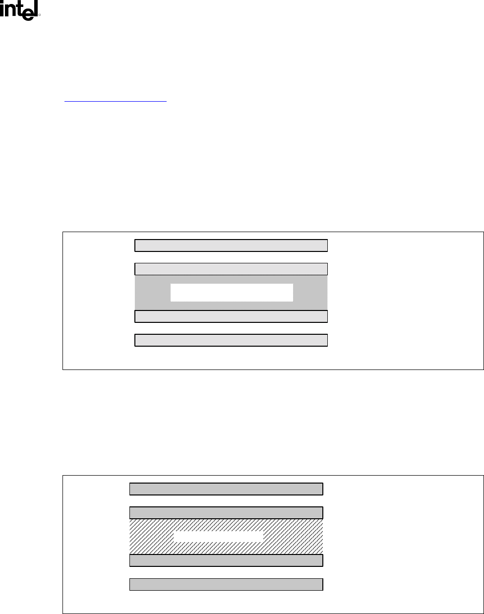
1. 7628 cloth (1-ply, 0.007 inch when cured with 40% resin) is the most popular and highest-volume in
PCB production today. This stack-up will make routing impossible.
• Fab construction (4 layers)
• Z
o
= 70 Ω ± 15%
Figure 99. 7 mil Stack-Up (Not Routable)
7mil_stackup
Total thickness
= 62 mils
Not Routable
Component-side layer: 0.5 oz. Cu
Ground layer 2: 1 oz. Cu
7-mil prepreg
Ground layer 3: 1 oz. Cu
Solder-side layer 4: 0.5 oz. Cu
7-mil prepreg
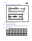
2. 2116 cloth (1-ply, 0.0045 inch when cured with 53% resin) is the second-highest-volume cloth in
production today. Because of the impedance and layout requirements of traces for Direct RDRAM,
AGP 2.0, and the hub interface, this stack-up is recommended for Intel 820E chipset platform design.
• Fab construction (4 layers)
• Z
o
= 60 Ω ± 10%
Figure 100. 4.5 mil Stack-Up
4.5mil_stackup.vsd
Total thickness
= 62 mils
~48-mil core
Component-side layer: 0.5 oz. Cu
Ground layer 2: 1 oz. Cu
4.5-mil prepreg
Ground layer 3: 1 oz. Cu
Solder-side layer 4: 0.5 oz. Cu
4.5-mil prepreg


