


Intel
®
820E Chipset
R
186 Design Guide
2.5 VBSY
The 2.5 V
SBY
power plane is used to power the RDRAM core and the VCMOS rail on the RDRAMs.
The RDRAM core requires an approximately 4.5-A
maximum average DC current at 2.5 V. In the Intel
820E chipset reference board, the
2.5 V
SBY
plane is derived from the 5 V dual power plane using a
switching regulator. During the maximum load-step of 2 A, the maximum voltage fluctuation must be
less than 50 mV. The maximum tolerance for 2.5 V is 125 mV. However, during any 10 µs period, the
voltage cannot fluctuate more than 50 mV. The high-frequency bypassing requirements are satisfied
using capacitors on the RIMM itself. Low-frequency bypass requirements vary depending on the voltage
regulator used. By using a switching regulator with a relatively slow response time, the low-frequency
bypass recommendation is eight 100 µF bulk capacitors (0.1-
Ω ESR) near the RIMM connectors. By
using a linear regulator with a substantially faster response time, the low-frequency bypass requirement
could be reduced.
The
VCMOS rail requires a maximum of 3 mA at 1.8 V. This rail must be powered during Suspend to
RAM
. Therefore, the VCMOS rail cannot be connected to the MCH core power. Because the current
requirements of
VCMOS are so low, a resistor divider can be used to generate VCMOS from 2.5 V
SBY
.
The resistor divider should be 36
Ω (top) / 100 Ω (bottom). Additionally, it should be bypassed with a
0.1-
µF chip capacitor.
The Intel reference board uses a switching regulator from
5 V dual. It may be possible to use a linear
regulator to regulate from 3.3 V
SB
. However, the thermal characteristics must be considered.
Additionally, a
low-dropout linear regulator would be necessary. If 2.5 V
SBY
is regulated from 3.3 V
SB
,
the 3.3 V
SB
regulator must be able to supply enough current for all the 3.3 V
SB
device requirements as
well as
the 2.5 V
SBY
requirements.
Refer to the 1.8 V power plane information for 1.8 V and 2.5 V power sequencing requirements.
Note: This regulator is required in all designs. However, in systems that do not support STR, the 2.5 V rail is
powered from either the 3.3 V or 5 V core well.
1.8 V
The 1.8 V plane powers the MCH core, the ICH2 hub interface’s I/O buffers, and the RDRAM
termination resistors. This power plane has a total power requirement of approximately 1.7 A. The 1.8 V
plane should be decoupled with a 0.1 µF and 0.01 µF chip capacitor at
each corner of the MCH and with
a single 1 µF and 0.1 µF capacitor at the ICH2.
Note: This regulator is required in all designs.
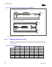
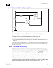
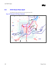
Power
must not be applied to the RDRAM termination resistors (V
TERM
) before applying power to the
RDRAM core (2.5 V
SBY
in this design). This can be guaranteed by placing a Schottky diode between
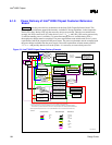
1.8 V and 2.5 V, as shown in the Figure 102: