Intel
®
820E Chipset
R
158 Design Guide
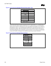
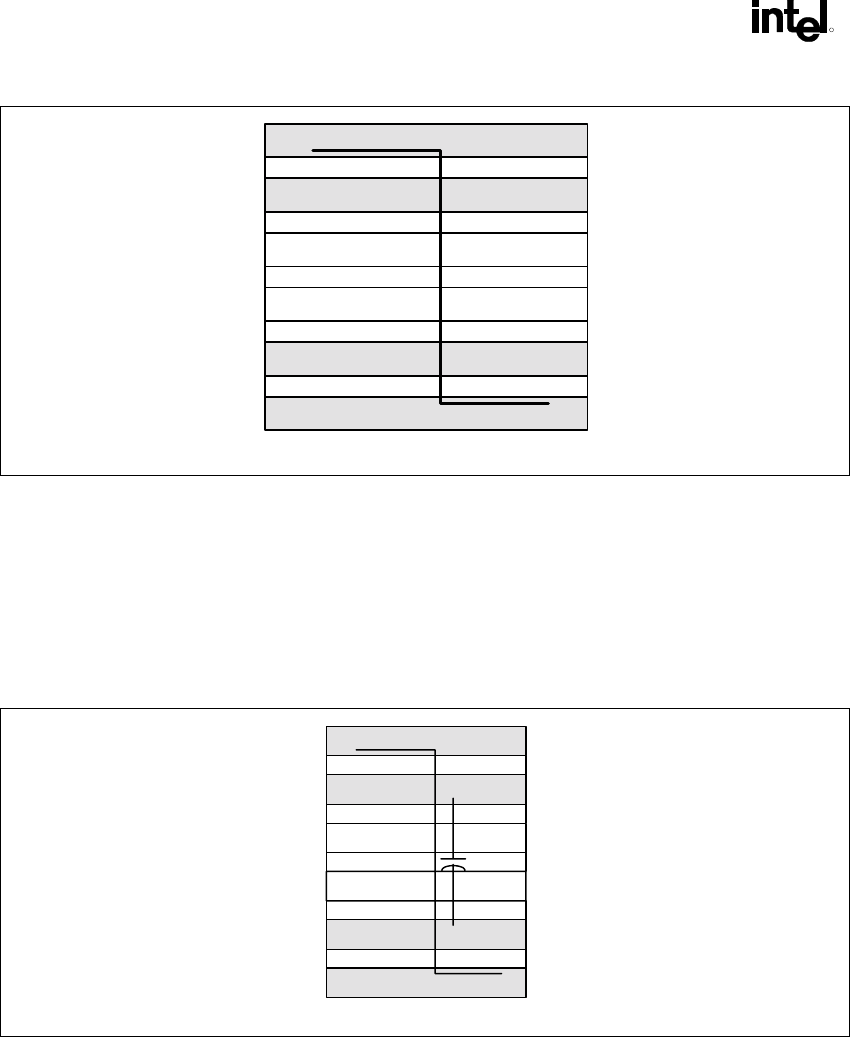
Figure 81. Layer Switch with Multiple Reference Planes (Same Type)
lay_sw_mult_refplane
Signal Layer A
Signal Layer B
Layer
Layer
Ground Plane
Ground Plane
When routing and stack-up constraints require that an AGTL+ signal reference V
CC
or multiple planes,
special care must be taken to minimize the SSO effect on timing and noise margin. The best method of
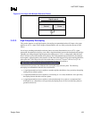
reducing adverse effects is to add high-frequency decoupling wherever the transitions occur, as shown in
the following two figures. Again, such decoupling should be in the vicinity of the signal transition via
and should use capacitors with minimal effective series resistance (ESR) and effective series inductance
(ESL). When placing the caps, it is advisable to space the V
SS
and V
CC
vias as closely as possible and/or
use dual vias, since the via inductance may sometimes exceed the actual capacitor inductance.
Figure 82. Layer Switch with Multiple Reference Planes
lay_sw_mult_refplane
Signal Layer A
Ground Plane
Power Plane
Signal Layer B
Layer
Layer


